SLLSEB3C March 2012 – November 2016 SN65LVPE502A
PRODUCTION DATA.
- 1 Features
- 2 Applications
- 3 Description
- 4 Revision History
- 5 Pin Configuration and Functions
- 6 Specifications
- 7 Parameter Measurement Information
- 8 Detailed Description
- 9 Application and Implementation
- 10Power Supply Recommendations
- 11Layout
- 12Device and Documentation Support
- 13Mechanical, Packaging, and Orderable Information
Package Options
Mechanical Data (Package|Pins)
Thermal pad, mechanical data (Package|Pins)
- RGE|24
Orderable Information
1 Features
- Single-Lane USB 3.0 Redriver and Equalizer
- Selectable Equalization, De-Emphasis and Output Swing Control
- Integrated Termination
- Hot-Plug Capable
- Low Active Power (U0 state):
- 315 mW (Typical), VCC = 3.3 V
- USB 3.0 Low Power Support:
- 7 mW (Typical) When No Connection Detected
- 70 mW (Typical) When Link in U2/U3 Mode
- Excellent Jitter and Loss Compensation Capability:
- >40 in of Total 4 mil Stripline on FR4
- Small Footprint, 3 mm × 3 mm and 4 mm × 4 mm, 24-Pin VQFN Packages
- High Protection Against ESD Transient:
- HBM: 5,000 V
- CDM: 1,500 V
- MM: 200 V
2 Applications
- Notebooks
- Desktops
- Docking Stations
- Backplanes
- Active Cables
3 Description
The SN65LVPE502x devices are dual-channel, single-lane USB 3.0 redriver and signal conditioners supporting data rates of 5 Gbps. The devices comply with USB 3.0 specification revision 1.0 supporting electrical idle condition and low frequency periodic signals (LFPS) for USB 3.0 power management modes.
Device Information(1)
| PART NUMBER | PACKAGE | BODY SIZE (NOM) |
|---|---|---|
| SN65LVPE502A | RLL (24) | 3.00 mm × 3.00 mm |
| SN65LVPE502A, SN65LVPE502B |
RGE (24) | 4.00 mm × 4.00 mm |
- For all available packages, see the orderable addendum at the end of the data sheet.
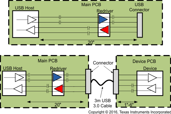
Typical Application
