SLLSEB3C March 2012 – November 2016 SN65LVPE502A
PRODUCTION DATA.
- 1 Features
- 2 Applications
- 3 Description
- 4 Revision History
- 5 Pin Configuration and Functions
- 6 Specifications
- 7 Parameter Measurement Information
- 8 Detailed Description
- 9 Application and Implementation
- 10Power Supply Recommendations
- 11Layout
- 12Device and Documentation Support
- 13Mechanical, Packaging, and Orderable Information
Package Options
Mechanical Data (Package|Pins)
Thermal pad, mechanical data (Package|Pins)
- RGE|24
Orderable Information
9 Application and Implementation
NOTE
Information in the following applications sections is not part of the TI component specification, and TI does not warrant its accuracy or completeness. TI’s customers are responsible for determining suitability of components for their purposes. Customers should validate and test their design implementation to confirm system functionality.
9.1 Application Information
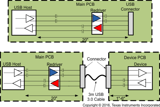
One example of the SN65LVPE502x used in a Host application on transmit and receive channels is shown in Typical Application. The redriver is required on the PCB path to pass transmitter compliance due to loss between the Host and connector. The redriver uses its equalization to recover the insertion loss and re-drive the signal with boosted swing down the remaining channel, through the USB 3.0 cable, and into the device PCB. Additionally on the receiver path, the SN65LVPE502x compensated for the Host to pass receiver jitter tolerance. The redriver recovers the loss from the device PCB, connector, and USB 3.0 cable and redrives the signal going into the Host receiver. The equalization, output swing, and de-emphasis settings are dependent upon the type of USB 3.0 signal path and end application.
9.2 Typical Application
 Figure 31. Typical Application Schematic
9.2.1 Design Requirements
Table 6 lists the parameters for this example.
Table 6. Application Parameters
| PARAMETER | VALUE |
|---|---|
| Input voltage range | 100 mV to 1200 mV |
| Output voltage range | 1050 mV to 1200 mV |
| Equalization | 0, 7, 15 bD (2.5 Gbps) |
| De-emphasis | 0, –3, –5 dB (OS floating) |
| VCC | 3.3-V nominal supply |
9.2.2 Detailed Design Procedure
The SN65LVPE502x is placed in the Host side and connected to a USB3 Type-A connector. The EQ and DE terminals must be pulled up, pulled down, or left floating depending on the amount of equalization or de-emphasis that is desired. The OS terminal must be pulled down or left floating depending on the required output swing. This device has terminals to be exclusively connected to the Host and to the device accordingly. In this Host side (even though the RX and TX pairs must be AC-coupled), this is an embedded implementation and Figure 31 only shows the AC-coupling capacitors on the TX pair to follow the convention.
To begin the design process, determine the following:
- Equalization (EQ) setting
- De-emphasis (DE) setting
- Output swing amplitude (OS) setting
The equalization must be set based on the insertion loss in the pre-channel (channel before the SN65LVPE502x device). The input voltage to the device is able to have a large range because of the receiver sensitivity and the available EQ settings. The EQ terminal can be pulled high through a resistor to VCC, low through a resistor to ground, or left floating. The de-emphasis setting must be set based on the length and characteristics of the post channel (channel after the SN65LVPE502x device). Output de-emphasis can be tailored using the DE terminal. This terminal must be pulled high through a resistor to VCC, low through a resistor to ground, or left floating. The output swing setting can also be configured based on the amplitude requirement to pass the compliance test. This setting is also based on the length of interconnect or cable the SN65LVPE502x is driving. This terminal must be pulled low through a resistor to ground or left floating.
9.2.3 Application Curves

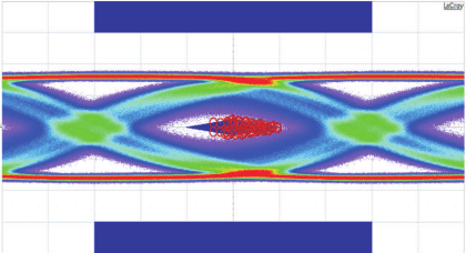
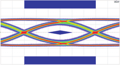
pre-channel = 20 in., and post-channel = 4 in. plus 3-m cable
With No Equalization

pre-channel = 20 in., and post-channel = 4 in. plus 3-m cable