SLLSEB3C March 2012 – November 2016 SN65LVPE502A
PRODUCTION DATA.
- 1 Features
- 2 Applications
- 3 Description
- 4 Revision History
- 5 Pin Configuration and Functions
- 6 Specifications
- 7 Parameter Measurement Information
- 8 Detailed Description
- 9 Application and Implementation
- 10Power Supply Recommendations
- 11Layout
- 12Device and Documentation Support
- 13Mechanical, Packaging, and Orderable Information
Package Options
Mechanical Data (Package|Pins)
Thermal pad, mechanical data (Package|Pins)
Orderable Information
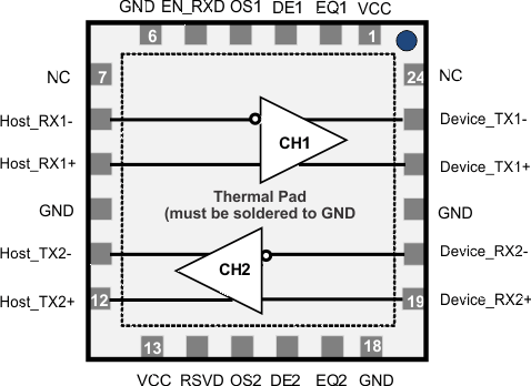
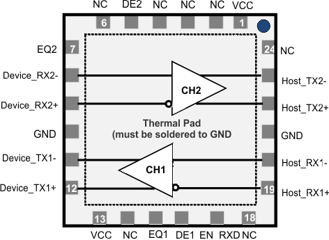
5 Pin Configuration and Functions
SN65LVPE502A RGE Package
24-Pin VQFN With Exposed Thermal Pad
Top View

SN65LVPE502B RGE Package
24-Pin VQFN With Exposed Thermal Pad
Top View

Pin Functions – RGE Packages
| PIN | TYPE(1) | DESCRIPTION | ||
|---|---|---|---|---|
| NAME | SN65LVPE502A | SN65LVPE502B | ||
| HIGH SPEED DIFFERENTIAL I/O PINS | ||||
| Host_RX1– | 8 | 20 | I | CML, inverting differential input for CH1. This pin is tied to an internal voltage bias by dual termination resistor circuit. Must connect to the USB 3.0 host side. |
| Host_RX1+ | 9 | 19 | I | CML, noninverting differential input for CH1. This pin is tied to an internal voltage bias by dual termination resistor circuit. Must connect to the USB 3.0 host side. |
| Device_RX2– | 20 | 8 | I | CML, inverting differential input for CH2. This pin is tied to an internal voltage bias by dual termination resistor circuit. Must connect to the USB 3.0 Device side. |
| Device_RX2+ | 19 | 9 | I | CML, noninverting differential input for CH2. This pin is tied to an internal voltage bias by dual termination resistor circuit. Must connect to the USB 3.0 Device side. |
| Device_TX1– | 23 | 11 | O | CML, inverting differential output for CH1. This pin is tied to an internal voltage bias by termination resistors. Must connect to the USB 3.0 Device side. |
| Device_TX1+ | 22 | 12 | O | CML, noninverting differential output for CH1. This pin is tied to an internal voltage bias by termination resistors. Must connect to the USB 3.0 Device side. |
| Host_TX2– | 11 | 23 | O | CML, inverting differential output for CH2. This pin is tied to an internal voltage bias by termination resistors. Must connect to the USB 3.0 Host side. |
| Host_TX2+ | 12 | 22 | O | CML, noninverting differential output for CH2. This pin is tied to an internal voltage bias by termination resistors. Must connect to the USB 3.0 Host side. |
| DEVICE CONTROL PINS | ||||
| EN_RXD | 5 | 17 | I | LVCMOS, sets device operation modes per Table 4; internally pulled to VCC. |
| RSVD | 14 | — | I | LVCMOS; RSVD. Can be left as No-Connect. |
| NC | 7, 24 | 2, 3, 4, 6, 14, 18, 24 | — | Pads are not internally connected. |
| EQ CONTROL PINS(2) | ||||
| DE1, DE2 | 3, 16 | 16, 5 | I | LVCMOS, selects de-emphasis settings for CH1 and CH2 per Table 4; internally tied to VCC/2. |
| EQ1, EQ2 | 2, 17 | 15, 7 | I | LVCMOS, selects equalization settings for CH1 and CH2 per Table 4, internally tied to VCC/2. |
| OS1, OS2 | 4, 15 | — | I | LVCMOS, selects output amplitude for CH1 and CH2 per Table 4, internally tied to VCC/2. |
| POWER PINS(3) | ||||
| GND | 6, 10, 18, 21, Thermal Pad | 10, 21, Thermal Pad | P | Supply ground |
| VCC | 1,13 | 1, 13 | P | Positive supply; must be 3.3 V ±10% |
(1) I = Input, O = Output, P = Power
(2) Internally biased to VCC/2 with >200 kΩ pullup or pulldown. When pins are left as NC, board leakage at this pin pad must be <1 µA otherwise drive to Vcc/2 to assert mid-level state.
(3) For SN65LVPE502B, pins 10 and 21 must be connected to GND, while 6 and 18 may be NC. For SN65LVPE502A, TI recommends at least two of the four pins (6, 10, 18, 21) be connected to ground.
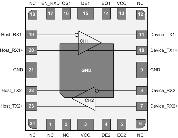
Pin Functions – RLL Package
| PIN | TYPE(1) | DESCRIPTION | |
|---|---|---|---|
| NAME | NO. | ||
| HIGH SPEED DIFFERENTIAL I/O PINS | |||
| Host_RX1– | 19 | I | CML, inverting differential input for CH1. This pin is tied to an internal voltage bias by dual termination resistor circuit. Must connect to the USB 3.0 host side. |
| Host_RX1+ | 20 | I | CML, noninverting differential input for CH1. This pin is tied to an internal voltage bias by dual termination resistor circuit. Must connect to the USB 3.0 host side. |
| Device_RX2– | 8 | I | CML, inverting differential input for CH2. This pin is tied to an internal voltage bias by dual termination resistor circuit. Must connect to the USB 3.0 Device side. |
| Device_RX2+ | 7 | I | CML, noninverting differential input for CH2. This pin is tied to an internal voltage bias by dual termination resistor circuit. Must connect to the USB 3.0 Device side. |
| Device_TX1– | 11 | O | CML, inverting differential output for CH1. This pin is tied to an internal voltage bias by termination resistors. Must connect to the USB 3.0 Device side. |
| Device_TX1+ | 10 | O | CML, noninverting differential output for CH1. This pin is tied to an internal voltage bias by termination resistors. Must connect to the USB 3.0 Device side. |
| Host_TX2– | 22 | O | CML, inverting differential output for CH2. This pin is tied to an internal voltage bias by termination resistors. Must connect to the USB 3.0 Host side. |
| Host_TX2+ | 23 | O | CML, noninverting differential output for CH2. This pin is tied to an internal voltage bias by termination resistors. Must connect to the USB 3.0 Host side. |
| DEVICE CONTROL PINS | |||
| EN_RXD | 17 | I | LVCMOS, sets device operation modes per Table 4; internally pulled to VCC. |
| NC | 1, 2, 6, 12, 18, 24 | — | Pads are not internally connected. |
| EQ CONTROL PINS(2) | |||
| DE1, DE2 | 15, 4 | I | LVCMOS, selects de-emphasis settings for CH1 and CH2 per Table 4; internally tied to VCC/2. |
| EQ1, EQ2 | 14, 5 | I | LVCMOS, selects equalization settings for CH1 and CH2 per Table 4; internally tied to VCC/2. |
| OS1, OS2 | 16, NC(3) | I | LVCMOS, selects output amplitude for CH1 and CH2 per Table 4; internally tied to VCC/2. |
| POWER PINS | |||
| GND | 9, Thermal Pad | P | Supply ground |
| VCC | 3 | P | Positive supply; must be 3.3 V ±10% |
(1) I = Input, O = Output, P = Power
(2) Internally biased to VCC/2 with >200 kΩ pullup or pulldown. When pins are left as NC, board leakage at this pin pad must be <1 µA otherwise drive to Vcc/2 to assert mid-level state.
(3) The SN65LVPE502A RLL package has OS2 internal no-connect to select the 1042-mVpp level on TX2.
