SLLSEB3C March 2012 – November 2016 SN65LVPE502A
PRODUCTION DATA.
- 1 Features
- 2 Applications
- 3 Description
- 4 Revision History
- 5 Pin Configuration and Functions
- 6 Specifications
- 7 Parameter Measurement Information
- 8 Detailed Description
- 9 Application and Implementation
- 10Power Supply Recommendations
- 11Layout
- 12Device and Documentation Support
- 13Mechanical, Packaging, and Orderable Information
Package Options
Mechanical Data (Package|Pins)
Thermal pad, mechanical data (Package|Pins)
- RGE|24
Orderable Information
6 Specifications
6.1 Absolute Maximum Ratings
over operating free-air temperature range (unless otherwise noted)(1)| MIN | MAX | UNIT | ||
|---|---|---|---|---|
| Supply voltage, VCC(2) | –0.5 | 4 | V | |
| Voltage | Differential I/O | –0.5 | 4 | V |
| Control I/O | –0.5 | VCC + 0.5 | V | |
| Continuous power dissipation | See Dissipation Ratings | |||
| Storage temperature, Tstg | –65 | 150 | °C | |
(1) Stresses beyond those listed under Absolute Maximum Ratings may cause permanent damage to the device. These are stress ratings only, which do not imply functional operation of the device at these or any other conditions beyond those indicated under Recommended Operating Conditions. Exposure to absolute-maximum-rated conditions for extended periods may affect device reliability.
(2) All voltage values, except differential voltages, are with respect to network ground terminal.
6.2 ESD Ratings
| VALUE | UNIT | |||
|---|---|---|---|---|
| V(ESD) | Electrostatic discharge | Human-body model (HBM), per ANSI/ESDA/JEDEC JS-001(1) | ±5000 | V |
| Charged-device model (CDM), per JEDEC specification JESD22-C101(2) | ±1500 | |||
| Machine model(3) | ±200 | |||
(1) Tested in accordance with JEDEC Standard 22, Test Method A114-B
(2) Tested in accordance with JEDEC Standard 22, Test Method C101-A
(3) Tested in accordance with JEDEC Standard 22, Test Method A115-A
6.3 Recommended Operating Conditions
| MIN | TYP | MAX | UNIT | |||
|---|---|---|---|---|---|---|
| VCC | Supply voltage | 3 | 3.3 | 3.6 | V | |
| CCOUPLING | AC-coupling capacitor | 75 | 200 | nF | ||
| TA | Operating free-air temperature | –40 | 85 | °C | ||
| DEVICE PARAMETERS | ||||||
| ICCCCCC | Supply current | EN_RXD, RSVD, EQ cntrl = NC, K28.5 pattern at 5 Gbps, VID = 1000 mVpp |
100 | 120 | mA | |
| ICCRX.Detect | Supply current | In RX.Detect mode | 2 | 5 | mA | |
| ICCsleep | Supply current | EN_RXD = GND | 0.01 | 0.1 | mA | |
| ICCU2-U3 | Supply current | Link in USB low power state | 21 | mA | ||
| Maximum data rate | 5 | Gbps | ||||
| tENB | Device enable time | Sleep mode exit time EN_RXD L → H with RX termination present |
100 | µs | ||
| tDIS | Device disable time | Sleep mode entry time EN_RXD H → L | 2 | µs | ||
| TRX.DETECT | RX.Detect start event | Power-up time | 100 | µs | ||
| CONTROL LOGIC | ||||||
| VIH | High-level input voltage | 2.8 | VCC | V | ||
| VIL | Low-level input voltage | –0.3 | 0.5 | V | ||
| VHYS | Input hysteresis | 150 | mV | |||
| IIH | High level input current | OSx, EQx, DEx = VCC | 30 | µA | ||
| EN_RXD = VCC | 1 | |||||
| RSVD = VCC | 30 | |||||
| IIL | Low level input current | OSx, EQx, DEx = GND | –30 | µA | ||
| EN_RXD = GND | –30 | |||||
| RSVD = GND | –1 | |||||
6.4 Thermal Information
| THERMAL METRIC(1) | SN65LVPE502A, SN65LVPE502B | UNIT | ||
|---|---|---|---|---|
| RGE (VQFN) | RLL (VQFN) | |||
| 24 PINS | 24 PINS | |||
| RθJA | Junction-to-ambient thermal resistance | 46 | 41.6 | °C/W |
| RθJC(top) | Junction-to-case (top) thermal resistance | 42 | 43.2 | °C/W |
| RθJB | Junction-to-board thermal resistance | 13 | 11.5 | °C/W |
| ψJT | Junction-to-top characterization parameter | 4 | 6.3 | °C/W |
| ψJB | Junction-to-board characterization parameter | — | 1.1 | °C/W |
| RθJC(bot) | Junction-to-case (bottom) thermal resistance | — | 11.5 | °C/W |
(1) For more information about traditional and new thermal metrics, see the Semiconductor and IC Package Thermal Metrics application report.
6.5 Electrical Characteristics
over recommended operating conditions (unless otherwise noted)| PARAMETER | TEST CONDITIONS | MIN | TYP | MAX | UNIT | |
|---|---|---|---|---|---|---|
| RECEIVER AC/DC | ||||||
| Vindiff_pp | RX1, RX2 input voltage swing | AC-coupled differential RX peak-to-peak signal | 100 | 1200 | mVpp | |
| VCM_RX | RX1, RX2 common mode voltage | 3.3 | V | |||
| VinCOM_P | RX1, RX2 AC peak common mode voltage | Measured at RX pins with termination enabled | 150 | mVpp | ||
| ZCM_RX | DC common mode impedance | 18 | 26 | 30 | Ω | |
| Zdiff_RX | DC differential input impedance | 72 | 80 | 120 | Ω | |
| ZRX_High_IMP+ | DC Input high impedance | Device in sleep mode RX termination not powered measured with respect to GND over 500 mV maximum | 50 | 85 | kΩ | |
| VRX-LFPS-DET-PP | Low frequency periodic signaling (LFPS) detect threshold | Measured at receiver pin, below minimum output is squelched, above maximum input signal is passed to output | 100 | 300 | mVpp | |
| RLRX-DIFF | Differential return loss | 50 MHz to 1.25 GHz | 10 | 11 | dB | |
| 1.25 GHz to 2.5 GHz | 6 | 7 | ||||
| RLRX-CM | Common mode return loss | 50 MHz to 2.5 GHz | 11 | 13 | dB | |
| TRANSMITTER AC/DC | ||||||
| VTXDIFF_TB-PP | Differential peak-to-peak output voltage, transition bit (VID = 800, 1200 mVpp, 5 Gbps) | RL = 100 Ω ±1%, DEx, OSx = NC | 800 | 1042 | 1200 | mV |
| RL = 100 Ω ±1%, DEx = NC, OSx = GND | 908 | |||||
| RL = 100 Ω ±1%, DEx = NC, OSx = VCC | 1127 | |||||
| VTXDIFF_NTB-PP | Differential peak-to-peak output voltage, non-transition bit (VID = 800, 1200 mVpp, 5 Gbps) | RL = 100 Ω ±1%, DEx = NC, OSx = 0, 1, NC | 1042 | mV | ||
| RL = 100 Ω ±1%, DEx = 0, OSx = 0, 1, NC | 661 | |||||
| RL = 100 Ω ±1%, DEx = 1, OSx = 0, 1, NC | 507 | |||||
| DE | De-emphasis level OS1, 2 = NC (for OS1, 2 = 1 and 0, see Table 4) |
DE1/DE2 = NC | 0 | dB | ||
| DE1/DE2 = 0 (SN65LVPE502A, RLL package) | –3.5 | |||||
| DE1/DE2 = 0 (SN65LVPE502x, RGE packages) | –3 | –3.5 | –4 | |||
| DE1/DE2 = 1 | –6 | |||||
| TDE | De-emphasis width | 0.85 | UI | |||
| Zdiff_TX | DC differential impedance | 72 | 90 | 120 | Ω | |
| ZCM_TX | DC common mode impedance | Measured w.r.t to AC ground over 0 V to 500 mV | 18 | 23 | 30 | Ω |
| RLdiff_TX | Differential return loss | f = 50 MHz to 1.25 GHz | 9 | 10 | dB | |
| f = 1.25 GHz to 2.5 GHz | 6 | 7 | ||||
| RLCM_TX | Common mode return loss | f = 50 MHz to 2.5 GHz | 11 | 12 | dB | |
| ITX_SC | TX short circuit current | TX± shorted to GND | 60 | mA | ||
| VTX_CM_DC | Transmitter DC common mode voltage | OSx = NC | 2 | 2.6 | 3 | V |
| VTX_CM_AC_Active | TX AC common mode voltage active | 30 | 100 | mVpp | ||
| VTX_idle_diff-ACpp | Electrical idle differential peak to peak output voltage | HPF to remove DC | 0 | 10 | mVpp | |
| VTX_CM_DeltaU1-U0 | Absolute delta of DC CM voltage during active and idle states | 35 | 200 | mV | ||
| VTX_idle_diff-DC | DC Electrical idle differential output voltage | Voltage must be low pass filtered to remove any AC component | 0 | 10 | mV | |
| Vdetect | Voltage change to allow receiver detect | Positive voltage to sense receiver termination | 600 | mV | ||
| tR, tF | Output rise and fall time | 20% to 80% of differential voltage measured 1 in. from the output pin | 30 | 65 | ps | |
| tRF_MM | Output rise and fall time mismatch | 20% to 80% of differential voltage measured 1 in. from the output pin | 1.5 | 20 | ps | |
| Tdiff_LH, Tdiff_HL | Differential propagation delay | De-emphasis = –3.5 dB (CH 0 and CH 1), propagation delay between 50% level at input and output | 305 | 370 | ps | |
| tidleEntry, tidleExit | Idle entry and exit times | See Figure 2 | 4 | 6 | ns | |
| CTX | TX input capacitance to GND | At 2.5 GHz | 1.25 | pF | ||
| JITTER | ||||||
| TTX-EYE(1)(2) | Total jitter (Tj) at point A | Device setting: OS1 = L, DE1 = –6 dB, EQ1 = 7 dB | 0.23 | 0.5 | UIpp(4) | |
| DJTX(2) | Deterministic jitter (Dj) | Device setting: OS1 = L, DE1 = –6 dB, EQ1 = 7 dB | 0.14 | 0.3 | UIpp(4) | |
| RJTX(2)(3) | Random jitter (Rj) | Device setting: OS1 = L, DE1 = –6 dB, EQ1 = 7 dB | 0.08 | 0.2 | UIpp(4) | |
| TTX-EYE(1)(2) | Total jitter (Tj) at point B | Device setting: OS2 = H, DE2 = –6 dB, EQ2 = 7 dB | 0.15 | 0.5 | UIpp(4) | |
| DJTX(2) | Deterministic jitter (Dj) | Device setting: OS2 = H, DE2 = –6 dB, EQ2 = 7 dB | 0.07 | 0.3 | UIpp(4) | |
| RJTX(2)(3) | Random jitter (Rj) | Device setting: OS2 = H, DE2 = –6 dB, EQ2 = 7 dB | 0.08 | 0.2 | UIpp(4) | |
(1) Includes RJ at 10–12 BER.
(2) Deterministic jitter measured with K28.5 pattern and Random jitter measured with K28.5 pattern at the ends of reference channel in Figure 5, VID = 1000 mVpp, 5 Gbps, and –3.5 dB DE from source.
(3) Rj calculated as 14.069 times the RMS random jitter for 10–12 BER.
(4) UI = 200 ps
6.6 Dissipation Ratings
over recommended operating free-air temperature range (unless otherwise noted)| PARAMETER | TEST CONDITIONS | MIN | TYP | MAX(1) | UNIT | |
|---|---|---|---|---|---|---|
| PD | Device power dissipation | RSVD, EN_RXD, EQ cntrl pins = NC, K28.5 pattern at 5 Gbps, VID = 1000 mVpp |
330 | 450 | mW | |
| PSlp | Device power dissipation in sleep mode | EN_RXD = GND | 0.03 | 0.4 | mW | |
(1) The maximum rating is simulated under 3.6 V VCC. Device power: the SN65LVPE502x is designed to operate from a single, 3.3-V supply.
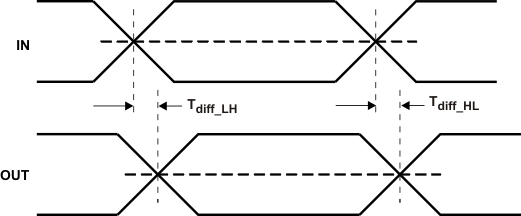 Figure 1. Propagation Delay
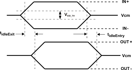 Figure 2. Electrical Idle Mode Exit and Entry Delay
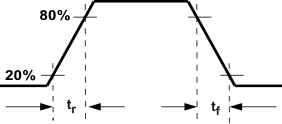 Figure 3. Output Rise and Fall Times
 Figure 4. Output De-Emphasis Levels OSx = NC
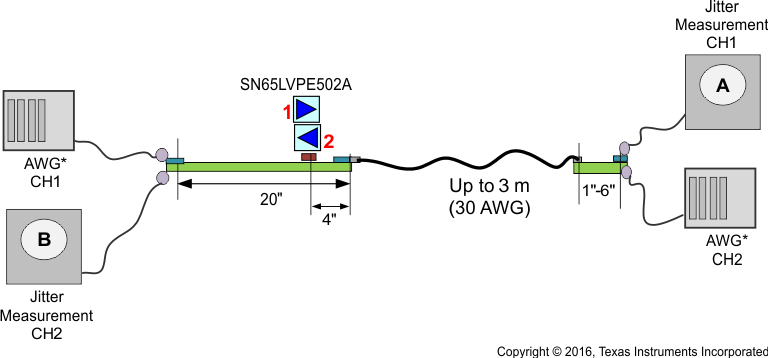 Figure 5. Jitter Measurement Setup

For more detailed placement example of redriver, see Typical Characteristics.
Figure 6. Redriver Placement Example
6.7 Typical Characteristics
Table 1. Case I Fixed Output and Variable Input Trace (3-m Cable)
| GRAPH TITLE | FIGURE |
|---|---|
| DE = 0 dB, EQ = 0 dB, Input = 4 in., Output = 4 in., and 3-m Cable | Figure 7 |
| DE = 0 dB, EQ = 0 dB, Input = 8 in., Output = 4 in., and 3-m Cable | Figure 8 |
| DE = 0 dB, EQ = 0 dB, Input = 12 in., Output = 4 in., and 3-m Cable | Figure 9 |
| DE = 0 dB, EQ = 0 dB, Input = 16 in., Output = 4 in., and 3-m Cable | Figure 10 |
| DE = 0 dB, EQ = 0 dB, Input = 20 in., Output = 4 in., and 3-m Cable | Figure 11 |
| DE = 0 dB, EQ = 7 dB, Input = 24 in., Output = 4 in., and 3-m Cable | Figure 12 |
| DE = 0 dB, EQ = 7 dB, Input = 32 in., Output = 4 in., and 3-m Cable | Figure 13 |
| DE = 0 dB, EQ = 7 dB, Input = 36 in., Output = 4 in., and 3-m Cable | Figure 14 |
| DE = 0 dB, EQ = 15 dB, Input = 36 in., Output = 4 in., and 3-m Cable | Figure 15 |
| DE = 0 dB, EQ = 15 dB, Input = 48 in., Output = 4 in., and 3-m Cable | Figure 16 |
Table 2. Case II Fixed Input and Variable Output Trace (3-m Cable)
| GRAPH TITLE | FIGURE |
|---|---|
| DE = 0 dB, EQ = 7 dB, Input = 12 in., Output = 4 in., and 3-m Cable | Figure 17 |
| DE = 0 dB, EQ = 7 dB, Input = 12 in., Output = 8 in., and 3-m Cable | Figure 18 |
| DE = 0 dB, EQ = 7 dB, Input = 12 in., Output = 12 in., and 3-m Cable | Figure 19 |
| DE = 0 dB, EQ = 7 dB, Input = 12 in., Output = 16 in., and 3-m Cable | Figure 20 |
| DE = 0 dB, EQ = 7 dB, Input = 12 in., Output = 20 in., and 3-m Cable | Figure 21 |
Table 3. Case III Fixed Input and Variable Output Trace (No Cable)
| GRAPH TITLE | FIGURE |
|---|---|
| DE = 0 dB, EQ = 7 dB, Input = 12 in., and Output = 8 in. | Figure 22 |
| DE = 0 dB, EQ = 7 dB, Input = 12 in., and Output = 32 in. | Figure 23 |
| DE = 0 dB, EQ = 7 dB, Input = 12 in., and Output = 36 in. | Figure 24 |
| DE = –3.5 dB, EQ = 7 dB, Input = 12 in., and Output = 36 in. | Figure 25 |
| DE = –6 dB, EQ = 7 dB, Input = 12 in., and Output = 40 in. | Figure 26 |
| DE = –6 dB, EQ = 7 dB, Input = 12 in., and Output = 44 in. | Figure 27 |
6.7.1 Case I – Fixed Output, Variable Input Trace, and 3-m Cable
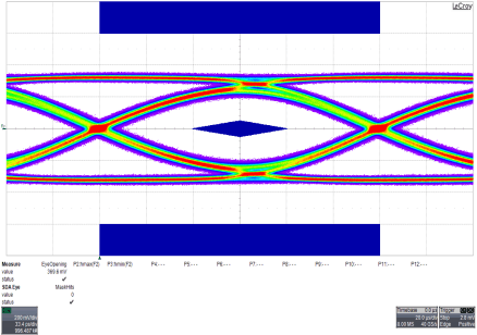 Figure 7. DE = 0 dB, EQ = 0 dB, Input = 4 in.,
Output = 4 in., and 3-m Cable
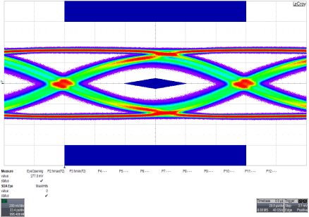 Figure 9. DE = 0 dB, EQ = 0 dB, Input = 12 in.,
Output = 4 in., and 3-m Cable
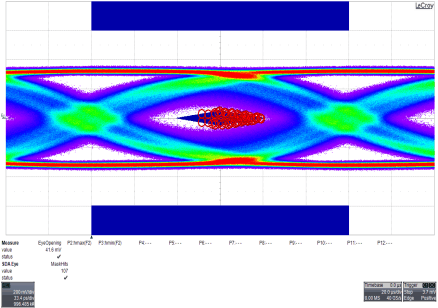 Figure 11. DE = 0 dB, EQ = 0 dB, Input = 20 in.,
Output = 4 in., and 3-m Cable
 Figure 13. DE = 0 dB, EQ = 7 dB, Input = 32 in.,
Output = 4 in., and 3-m Cable
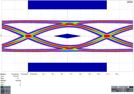 Figure 15. DE = 0 dB, EQ = 15 dB, Input = 36 in.,
Output = 4 in., and 3-m Cable
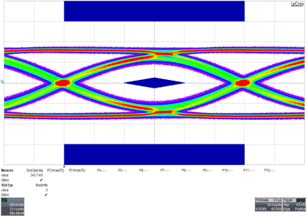 Figure 8. DE = 0 dB, EQ = 0 dB, Input = 8 in.,
Output = 4 in., and 3-m Cable
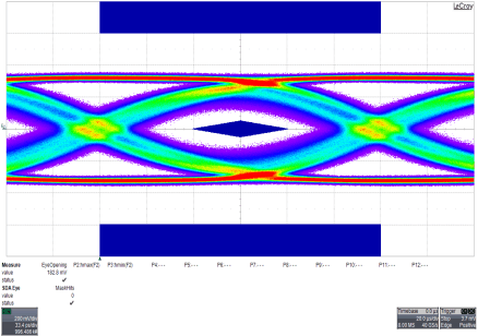 Figure 10. DE = 0 dB, EQ = 0 dB, Input = 16 in.,
Output = 4 in., and 3-m Cable
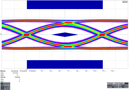 Figure 12. DE = 0 dB, EQ = 7 dB, Input = 24 in.,
Output = 4 in., and 3-m Cable
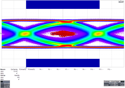 Figure 14. DE = 0 dB, EQ = 7 dB, Input = 36 in.,
Output = 4 in., and 3-m Cable
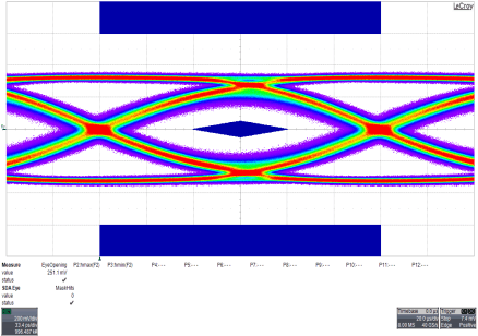 Figure 16. DE = 0 dB, EQ = 15 dB, Input = 48 in.,
Output = 4 in., and 3-m Cable
6.7.2 Case II – Fixed Input, Variable Output Trace, and 3-m Cable
 Figure 17. DE = 0 dB, EQ = 7 dB, Input = 12 in.,
Output = 4 in., and 3-m Cable
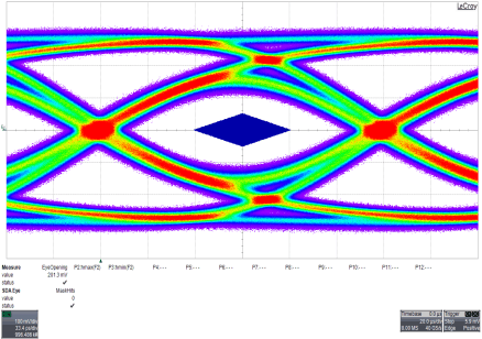 Figure 19. DE = 0 dB, EQ = 7 dB, Input = 12 in.,
Output = 12 in., and 3-m Cable
 Figure 21. DE = 0 dB, EQ = 7 dB, Input = 12 in., Output = 20 in., and 3-m Cable
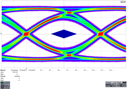 Figure 18. DE = 0 dB, EQ = 7 dB, Input = 12 in.,
Output = 8 in., and 3-m Cable
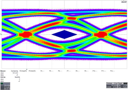 Figure 20. DE = 0 dB, EQ = 7 dB, Input = 12 in.,
Output = 16 in., and 3-m Cable
6.7.3 Case III – Fixed Input and Variable Output Trace (No Cable)
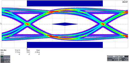 Figure 22. DE = 0 dB, EQ = 7 dB, Input = 12 in.,
and Output = 8 in.
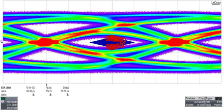 Figure 24. DE = 0 dB, EQ = 7 dB, Input = 12 in.,
and Output = 36 in.
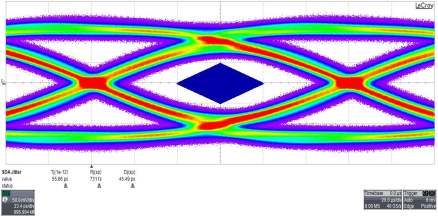 Figure 26. DE = –6 dB, EQ = 7 dB, Input = 12 in.,
and Output = 40 in.
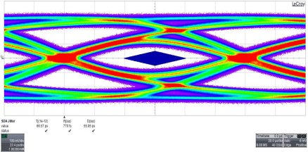 Figure 23. DE = 0 dB, EQ = 7 dB, Input = 12 in.,
and Output = 32 in.
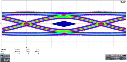 Figure 25. DE = –3.5 dB, EQ = 7 dB, Input = 12 in.,
and Output = 36 in.
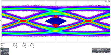 Figure 27. DE = –6 dB, EQ = 7 dB, Input = 12 in.,
and Output = 44 in.