SLASEV8 December   2020 TAS5822M

PRODUCTION DATA  

  1. Features
  2. Applications
  3. Description
  4. Revision History
  5. Pin Configuration and Functions
  6. Specifications
    1. 6.1 Absolute Maximum Ratings
    2. 6.2 ESD Ratings
    3. 6.3 Recommended Operating Conditions
    4. 6.4 Thermal Information
    5. 6.5 Electrical Characteristics
    6. 6.6 Timing Requirements
    7. 6.7 Typical Characteristics
      1. 6.7.1 Bridge Tied Load (BTL) Configuration Curves with 1SPW Modulation, Fsw = 768kHz
      2. 6.7.2 Parallel Bridge Tied Load (PBTL) Configuration Curves with 1SPW Modulation, Fsw = 768kHz
    8. 6.8 Parametric Measurement Information
      1. 6.8.1 Power Consumption Summary
  7. Detailed Description
    1. 7.1 Overview
    2. 7.2 Functional Block Diagram
    3. 7.3 Feature Description
      1. 7.3.1 Power Supplies
      2. 7.3.2 Device Clocking
      3. 7.3.3 Serial Audio Port – Clock Rates
      4. 7.3.4 Clock Halt Auto-recovery
      5. 7.3.5 Sample Rate on the Fly Change
      6. 7.3.6 Serial Audio Port - Data Formats and Bit Depths
      7. 7.3.7 Digital Audio Processing
      8. 7.3.8 Class D Audio Amplifier
        1. 7.3.8.1 Speaker Amplifier Gain Select
    4. 7.4 Device Functional Modes
      1. 7.4.1 Software Control
      2. 7.4.2 Speaker Amplifier Operating Modes
        1. 7.4.2.1 BTL Mode
        2. 7.4.2.2 PBTL Mode
      3. 7.4.3 Minimize EMI with Spread Spectrum
      4. 7.4.4 Minimize EMI with channel to channel phase shift
      5. 7.4.5 Minimize EMI with Multi-Devices PWM Phase Synchronization
      6. 7.4.6 Thermal Foldback
      7. 7.4.7 Device State Control
      8. 7.4.8 Device Modulation
        1. 7.4.8.1 BD Modulation
        2. 7.4.8.2 1SPW Modulation
        3. 7.4.8.3 Hybrid Modulation
    5. 7.5 Programming and Control
      1. 7.5.1 I2 C Serial Communication Bus
      2. 7.5.2 Slave Address
        1. 7.5.2.1 Random Write
        2. 7.5.2.2 Sequential Write
        3. 7.5.2.3 Random Read
        4. 7.5.2.4 Sequential Read
        5. 7.5.2.5 DSP Memory Book, Page and BQ update
        6. 7.5.2.6 Example Use
        7. 7.5.2.7 Checksum
          1. 7.5.2.7.1 Cyclic Redundancy Check (CRC) Checksum
          2. 7.5.2.7.2 Exclusive or (XOR) Checksum
      3. 7.5.3 Control via Software
        1. 7.5.3.1 Startup Procedures
        2. 7.5.3.2 Shutdown Procedures
        3. 7.5.3.3 Protection and Monitoring
          1. 7.5.3.3.1 Over current Shutdown (OCSD)
          2. 7.5.3.3.2 Speaker DC Protection
          3. 7.5.3.3.3 Device Over Temperature Protection
          4. 7.5.3.3.4 Over Voltage Protection
          5. 7.5.3.3.5 Under Voltage Protection
          6. 7.5.3.3.6 Clock Fault
    6. 7.6 Register Maps
      1. 7.6.1 CONTROL PORT Registers
  8. Application and Implementation
    1. 8.1 Application Information
    2. 8.2 Typical Applications
      1. 8.2.1 2.0 (Stereo BTL) System
      2. 8.2.2 MONO (PBTL) System
        1. 8.2.2.1 Design Requirements
        2. 8.2.2.2 Detailed Design Procedure
          1. 8.2.2.2.1 Bootstrap Capacitors
          2. 8.2.2.2.2 Inductor Selections
          3. 8.2.2.2.3 Power Supply Decoupling
          4. 8.2.2.2.4 Output EMI Filtering
        3. 8.2.2.3 Application Performance Plots
  9. Power Supply Recommendations
    1. 9.1 DVDD Supply
    2. 9.2 PVDD Supply
  10. 10Layout
    1. 10.1 Layout Guidelines
      1. 10.1.1 General Guidelines for Audio Amplifiers
      2. 10.1.2 Importance of PVDD Bypass Capacitor Placement on PVDD Network
      3. 10.1.3 Optimizing Thermal Performance
        1. 10.1.3.1 Device, Copper, and Component Layout
        2. 10.1.3.2 Stencil Pattern
          1. 10.1.3.2.1 PCB footprint and Via Arrangement
          2. 10.1.3.2.2 Solder Stencil
    2. 10.2 Layout Example
  11. 11Device and Documentation Support
    1. 11.1 Support Resources
    2. 11.2 Trademarks
    3. 11.3 Electrostatic Discharge Caution
    4. 11.4 Glossary
  12. 12Mechanical, Packaging, and Orderable Information

Package Options

Mechanical Data (Package|Pins)
Thermal pad, mechanical data (Package|Pins)
Orderable Information
Inductor Selections

It is required that the peak current is smaller than the OCP (Over current protection) value which is 7A (Typical) , there are 3 cases which cause high peak current flow through inductor.

  1. During power up (idle state, no audio input), the duty cycle increases from 0 to θ. There has a start-up current which flow through inductor to set up the common mode voltage (PVDD×θ).
    Note:

    θ = 0.5 (BD Modulation), 0.14 (1SPW Modulation), 0.14 (Hybrid Modulation)

    Table 8-2 shows the start-up current related to different Fsw, PVDD, Inductance and different PWM modulation scheme. Start-up current should within device's OCETHRES.

    Table 8-2 Start-up Current
    Modulation Scheme PVDD (V) FSW ((kHz)) LC filter Startup Peak Current (A)
    BD 13.5 384 4.7 µH + 0.68 µF 2.88
    10 µH + 0.68 µF 2
    768 4.7 µH + 0.68 µF 2.64
    10 µH + 0.68 µF 1.84
    18 384 4.7 µH + 0.68 µF 3.84
    10 µH + 0.68 µF 2.64
    768 4.7 µH + 0.68 µF 3.52
    10 µH + 0.68 µF 2.4
    24 384 4.7 µH + 0.68 µF 5.4
    10 µH + 0.68 µF 3.76
    768 4.7 µH + 0.68 µF 5
    10 µH + 0.68 µF 3.12
    1SPW 13.5 384 4.7 µH + 0.68 µF 1.28
    10 µH + 0.68 µF 0.96
    768 4.7 µH + 0.68 µF 1.12
    10 µH + 0.68 µF 0.72
    18 384 4.7 µH + 0.68 µF 1.84
    10 µH + 0.68 µF 1.2
    768 4.7 µH + 0.68 µF 1.52
    10 µH + 0.68 µF 1.04
    24 384 4.7 µH + 0.68 µF 2.6
    10 µH + 0.68 µF 1.6
    768 4.7 µH + 0.68 µF 2.4
    10 µH + 0.68 µF 1.36

    Figure 8-3 and Figure 8-4 shows how modulation scheme affect the start-up current. OUTP_PWM is Class D amplifier's PWM output, OUTP_FILTER is the common mode voltage on the capacitor of LC filter.

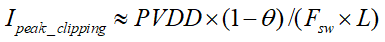
  2. During music playing, some audio burst signal (high frequency) with very hard PVDD clipping will cause PWM duty cycle increase dramatically. This is the worst case and it rarely happens.
    Equation 1. GUID-E11B7C12-0C20-443A-8A02-2A8C43D8D8B4-low.gif
  3. Peak current due to Max output power. Ignore the ripple current flow through capacitor.
    Equation 2. GUID-DBF931BB-4A55-4268-8B36-57FE37C38F13-low.gif

Same PVDD and switching frequency, larger inductance means smaller idle current for lower power dissipation. It's suggested that inductor's saturation current Isat, is larger than the amplifier's peak current during power-up and playing audio. In addition, the effective inductance at the peak current is required to be at least 80% of the inductance value in Table 8-3 to meet datasheet specifications.

Table 8-3 LC filter recommendation
Switching Frequency (kHz) Modulation Scheme Recommended Minimum Inductance (uH) for LC filter design
1024 1SPW 3.3 µH (or larger) + Capacitor (0.22uF~0.68uF)
768 4.7 µH (or larger) + Capacitor (0.22uF~0.68uF)
384 or 480 10 µH (or larger) +Capacitor (0.22uF~0.68uF)
384~1024 BD 8.2uH (or Larger) +Capacitor (0.22uF~0.68uF)