SPRSP62C December 2022 – November 2025 TDA4AL-Q1 , TDA4VE-Q1 , TDA4VL-Q1
PRODUCTION DATA
- 1
- 1 Features
- 2 Applications
- 3 Description
- 4 Device Comparison
-
5 Terminal Configuration and Functions
- 5.1 Pin Diagrams
- 5.2 Pin Attributes
- 5.3
Signal Descriptions
- 13
- 5.3.1 ADC
- 5.3.2 DDRSS
- 5.3.3 GPIO
- 5.3.4 I2C
- 5.3.5 I3C
- 5.3.6 MCAN
- 5.3.7 MCSPI
- 5.3.8 UART
- 5.3.9 MDIO
- 5.3.10 CPSW2G
- 5.3.11 ECAP
- 5.3.12 EQEP
- 5.3.13 EPWM
- 5.3.14 USB
- 5.3.15 Display Port
- 5.3.16 Hyperlink
- 5.3.17 PCIE
- 5.3.18 SERDES
- 5.3.19 DSI
- 5.3.20 CSI
- 5.3.21 MCASP
- 5.3.22 DMTIMER
- 5.3.23 CPTS
- 5.3.24 DSS
- 5.3.25 GPMC
- 5.3.26 MMC
- 5.3.27 OSPI
- 5.3.28 Hyperbus
- 5.3.29 Emulation and Debug
- 5.3.30 System and Miscellaneous
- 5.3.31 Power
- 5.4 Connection for Unused Pins
-
6 Specifications
- 6.1 Absolute Maximum Ratings
- 6.2 ESD Ratings
- 6.3 Recommended Operating Conditions
- 6.4 Power-On-Hour (POH) Limits
- 6.5 Operating Performance Points
- 6.6
Electrical Characteristics
- 6.6.1 I2C, Open-Drain, Fail-Safe (I2C OD FS) Electrical Characteristics
- 6.6.2 Fail-Safe Reset (FS Reset) Electrical Characteristics
- 6.6.3 HFOSC/LFOSC Electrical Characteristics
- 6.6.4 eMMCPHY Electrical Characteristics
- 6.6.5 SDIO Electrical Characteristics
- 6.6.6 CSI2/DSI D-PHY Electrical Characteristics
- 6.6.7 ADC12B Electrical Characteristics
- 6.6.8 LVCMOS Electrical Characteristics
- 6.6.9 USB2PHY Electrical Characteristics
- 6.6.10 SerDes 2-L-PHY/4-L-PHY Electrical Characteristics
- 6.6.11 UFS M-PHY Electrical Characteristics
- 6.6.12 eDP/DP AUX-PHY Electrical Characteristics
- 6.6.13 DDR0 Electrical Characteristics
- 6.7 VPP Specifications for One-Time Programmable (OTP) eFuses
- 6.8 Thermal Resistance Characteristics
- 6.9 Temperature Sensor Characteristics
- 6.10
Timing and Switching Characteristics
- 6.10.1 Timing Parameters and Information
- 6.10.2
Power Supply Sequencing
- 6.10.2.1 Power Supply Slew Rate Requirement
- 6.10.2.2 Combined MCU and Main Domains Power- Up Sequencing
- 6.10.2.3 Combined MCU and Main Domains Power- Down Sequencing - Option 1
- 6.10.2.4 Isolated MCU and Main Domains Power- Up Sequencing
- 6.10.2.5 Isolated MCU and Main Domains Power- Down Sequencing - Option 1
- 6.10.2.6 Independent MCU and Main Domains, Entry and Exit of MCU Only Sequencing
- 6.10.2.7 Independent MCU and Main Domains, Entry and Exit of DDR Retention State
- 6.10.2.8 Independent MCU and Main Domains, Entry and Exit of GPIO Retention Sequencing
- 6.10.3 System Timing
- 6.10.4
Clock Specifications
- 6.10.4.1 Input and Output Clocks / Oscillators
- 6.10.4.2 Output Clocks
- 6.10.4.3 PLLs
- 6.10.4.4 Module and Peripheral Clocks Frequencies
- 6.10.5
Peripherals
- 6.10.5.1 ATL
- 6.10.5.2
CPSW2G
- 6.10.5.2.1 CPSW2G MDIO Interface Timings
- 6.10.5.2.2 CPSW2G RMII Timings
- 6.10.5.2.3
CPSW2G RGMII Timings
- 6.10.5.2.3.1 RGMII[x]_RXC Timing Requirements – RGMII Mode
- 6.10.5.2.3.2 CPSW2G Timing Requirements for RGMII[x]_RD[3:0], and RGMII[x]_RCTL – RGMII Mode
- 6.10.5.2.3.3 CPSW2G RGMII[x]_TXC Switching Characteristics – RGMII Mode
- 6.10.5.2.3.4 RGMII[x]_TD[3:0], and RGMII[x]_TX_CTL Switching Characteristics – RGMII Mode
- 6.10.5.3 CSI-2
- 6.10.5.4 DDRSS
- 6.10.5.5 DSS
- 6.10.5.6 eCAP
- 6.10.5.7 EPWM
- 6.10.5.8 eQEP
- 6.10.5.9 GPIO
- 6.10.5.10 GPMC
- 6.10.5.11 HyperBus
- 6.10.5.12 I2C
- 6.10.5.13 I3C
- 6.10.5.14 MCAN
- 6.10.5.15 MCASP
- 6.10.5.16 MCSPI
- 6.10.5.17 MMCSD
- 6.10.5.18 CPTS
- 6.10.5.19 OSPI
- 6.10.5.20 PCIE
- 6.10.5.21 Timers
- 6.10.5.22 UART
- 6.10.5.23 USB
- 6.10.6 Emulation and Debug
-
7 Applications,
Implementation, and Layout
- 7.1 Device Connection and Layout Fundamentals
- 7.2 Peripheral- and Interface-Specific Design Information
- 8 Device and Documentation Support
- 9 Revision History
- 10Mechanical, Packaging, and Orderable Information
Package Options
Refer to the PDF data sheet for device specific package drawings
Mechanical Data (Package|Pins)
- ALZ|770
Thermal pad, mechanical data (Package|Pins)
Orderable Information
6.10.5.5 DSS
For more details about features and additional description information on the device Display Subsystem – Video Output Ports, see the corresponding sections within Signal Descriptions and Detailed Description.
Table 6-34 represents DPI timing conditions.
| PARAMETER | MIN | MAX | UNIT | |
|---|---|---|---|---|
| INPUT CONDITIONS | ||||
| SRI | Input slew rate | 1.44 | 26.4 | V/ns |
| OUTPUT CONDITIONS | ||||
| CL | Output load capacitance | 1.5 | 5 | pF |
| PCB CONNECTIVITY REQUIREMENTS | ||||
| td(Trace Mismatch Delay) | Propagation delay mismatch across all traces | 100 | ps | |
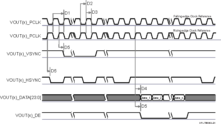
Table 6-35, Table 6-36, Figure 6-44 and Figure 6-45 assume testing over the recommended operating conditions and electrical characteristic conditions.
| NO.(2) | PARAMETER | MIN | MAX | UNIT | |
|---|---|---|---|---|---|
| D1 | tc(pclk) | Cycle time, VOUT(x)_PCLK | 6.06 | ns | |
| D2 | tw(pclkL) | Pulse duration, VOUT(x)_PCLK low | 0.475×P(1) | ns | |
| D3 | tw(pclkH) | Pulse duration, VOUT(x)_PCLK high | 0.475×P(1) | ns | |
| D4 | td(pclkV-dataV) | Delay time, VOUT(x)_PCLK transition to VOUT(x)_DATA[23:0] transition | -0.68 | 1.78 | ns |
| D5 | td(pclkV-ctrlL) | Delay time, VOUT(x)_PCLK transition to control signals VOUT(x)_VSYNC, VOUT(x)_HSYNC, VOUT(x)_DE falling edge | -0.68 | 1.78 | ns |

| NO.(2) | MIN | MAX | UNIT | ||
|---|---|---|---|---|---|
| D6 | tc(extpclkin) | Cycle time, VOUT(x)_EXTPCLKIN | 6.06 | ns | |
| D7 | tw(extpclkinL) | Pulse duration, VOUT(x)_EXTPCLKIN low | 0.45×P(1) | ns | |
| D8 | tw(extpclkinH) | Pulse duration, VOUT(x)_EXTPCLKIN high | 0.45×P(1) | ns | |
 Figure 6-45 DPI External
Pixel Clock Input
Figure 6-45 DPI External
Pixel Clock InputFor more information, see Display Subsystem (DSS) and Peripherals section in Peripherals chapter in the device TRM.