SBOS874D August 2017 – February 2021 THS4561
PRODUCTION DATA
- 1 Features
- 2 Applications
- 3 Description
- 4 Revision History
- 5 Device Comparison Table
- 6 Pin Configuration and Functions
-
7 Specifications
- 7.1 Absolute Maximum Ratings
- 7.2 ESD Ratings
- 7.3 Recommended Operating Conditions
- 7.4 Thermal Information
- 7.5 Electrical Characteristics: VS+ – VS– = 5 V to 12 V
- 7.6 Typical Characteristics: (VS+) – (VS–) = 12 V
- 7.7 Typical Characteristics: (VS+) – (VS–) = 5 V
- 7.8 Typical Characteristics: (VS+) – (VS–) = 3 V
- 7.9 Typical Characteristics: (VS+) – (VS–) = 3-V to 12-V Supply Range
-
8 Parameter Measurement Information
- 8.1 Example Characterization Circuits
- 8.2 Output Interface Circuit for DC-Coupled Differential Testing
- 8.3 Output Common-Mode Measurements
- 8.4 Differential Amplifier Noise Measurements
- 8.5 Balanced Split-Supply Versus Single-Supply Characterization
- 8.6 Simulated Characterization Curves
- 8.7 Terminology and Application Assumptions
- 9 Detailed Description
- 10Application and Implementation
- 11Power Supply Recommendations
- 12Layout
- 13Device and Documentation Support
- 14Mechanical, Packaging, and Orderable Information
Package Options
Mechanical Data (Package|Pins)
Thermal pad, mechanical data (Package|Pins)
Orderable Information
3 Description
The THS4561 fully differential
amplifier (FDA) offers a simple interface from single-ended sources to the
differential output required by precision analog-to-digital converters (ADCs).
Designed for a very low,
8-Hz, 1/f voltage noise corner
and low, 130-dB total harmonic distortion (THD) while consuming only a
775-µA quiescent current, the THS4561 is well suited
for power-sensitive data acquisition (DAQ) systems where high performance is
required with the best signal-to-noise ratio (SNR) and spurious-free dynamic range
(SFDR) through the amplifier and ADC combination.
The THS4561 features the required negative rail input when interfacing a DC-coupled, ground-centered, source signal to a single-supply, differential-input ADC. Low DC error and drift terms support the emerging high-speed and high-resolution successive approximation register (SAR) and delta-sigma (ΔΣ) ADC input requirements. A 2.85-V to 12.6-V supply range with a flexible output common-mode setting with low headroom to the supplies supports a wide range of ADC input and digital-to-analog converter (DAC) output requirements.
The THS4561 device is characterized for operation from –40°C to +125°C.
| PART NUMBER | PACKAGE(1) | BODY SIZE (NOM) |
|---|---|---|
| THS4561 | VSSOP (8) | 3.00 mm × 3.00 mm |
| WQFN (10) | 2.00 mm × 2.00 mm | |
| VQFN (16) | 3.00 mm × 3.00 mm |
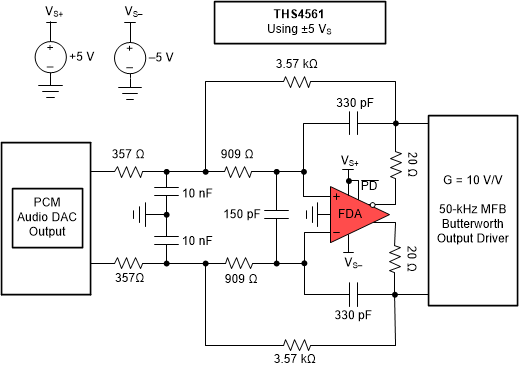
 Gain of 10 V/V PCM Audio DAC Output With
Second-Order MFB Filter at 50 kHz
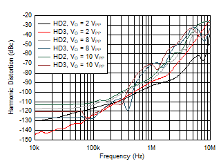
 Harmonic Distortion vs
Frequency