SBOS833R October 2017 – November 2021 TLV9001 , TLV9002 , TLV9004
PRODUCTION DATA
- 1
- 1 Features
- 2 Applications
- 3 Description
- 4 Revision History
- 5 Device Comparison Table
- 6 Pin Configuration and Functions
-
7 Specifications
- 7.1 Absolute Maximum Ratings
- 7.2 ESD Ratings
- 7.3 Recommended Operating Conditions
- 7.4 Thermal Information: TLV9001
- 7.5 Thermal Information: TLV9001S
- 7.6 Thermal Information: TLV9002
- 7.7 Thermal Information: TLV9002S
- 7.8 Thermal Information: TLV9004
- 7.9 Thermal Information: TLV9004S
- 7.10 Electrical Characteristics
- 7.11 Typical Characteristics
- 8 Detailed Description
- 9 Application and Implementation
- 10Power Supply Recommendations
- 11Layout
- 12Device and Documentation Support
- 13Mechanical, Packaging, and Orderable Information
Package Options
Mechanical Data (Package|Pins)
Thermal pad, mechanical data (Package|Pins)
- DPW|5
Orderable Information
9.2.1.2 Detailed Design Procedure
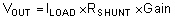
The transfer function of the circuit in Figure 9-1 is given in Equation 1.
The load current (ILOAD) produces a voltage drop across the shunt resistor (RSHUNT). The load current is set from 0 A to 1 A. To keep the shunt voltage below 100 mV at maximum load current, the largest shunt resistor is shown using Equation 2.
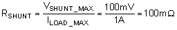
Using Equation 2, RSHUNT is calculated to be 100 mΩ. The voltage drop produced by ILOAD and RSHUNT is amplified by the TLV900x to produce an output voltage of approximately 0 V to 4.9 V. The gain needed by the TLV900x to produce the necessary output voltage is calculated using Equation 3.
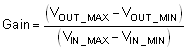
Using Equation 3, the required gain is calculated to be 49 V/V, which is set with resistors RF and RG. Equation 4 sizes the resistors RF and RG, to set the gain of the TLV900x to 49 V/V.

Selecting RF as 57.6 kΩ and RG as 1.2 kΩ provides a combination that equals 49 V/V. Figure 9-2 shows the measured transfer function of the circuit shown in Figure 9-1. Notice that the gain is only a function of the feedback and gain resistors. This gain is adjusted by varying the ratio of the resistors and the actual resistors values are determined by the impedance levels that the designer wants to establish. The impedance level determines the current drain, the effect that stray capacitance has, and a few other behaviors. There is no optimal impedance selection that works for every system, you must choose an impedance that is ideal for your system parameters.