SCDS423 October 2020 TMUX1575
PRODUCTION DATA
- 1 Features
- 2 Applications
- 3 Description
- 4 Revision History
- 5 Pin Configuration and Functions
- 6 Specifications
- 7 Parameter Measurement Information
- 8 Detailed Description
- 9 Application and Implementation
- 10Power Supply Recommendations
- 11Layout
- 12Device and Documentation Support
- 13Mechanical, Packaging, and Orderable Information
Package Options
Mechanical Data (Package|Pins)
- YCJ|16
Thermal pad, mechanical data (Package|Pins)
Orderable Information
3 Description
The TMUX1575 is a complementary metal-oxide semiconductor (CMOS) switch in a 2:1 (SPDT) configuration with 4-channels. The small size and operating supply voltage of 1.08 V to 3.6 V allows for use in a broad array of applications from servers and communication equipment to personal electronics applications. The device supports bidirectional analog and digital signals on the source (SxA, SxB) and drain (Dx) pins and can pass signals up to VDD x 2 with a maximum input/output voltage of 3.6 V.
Powered-off protection on the signal path of the TMUX1575 provides isolation when the supply voltage is removed (VDD = 0 V). Without this protection feature, switches can back-power the supply rail through an internal ESD diode and cause potential damage to the system.
Fail-safe logic circuitry allows voltages on the logic control pins to be applied before the supply pin, protecting the device from potential damage. All control inputs have 1.2 V logic compatible thresholds, eliminating the need for external logic translation. Integrated pull down resistor on the logic pins removes external components to reduce system size and cost.
| PART NUMBER | PACKAGE | BODY SIZE (NOM) |
|---|---|---|
| TMUX1575 | WCSP (16) | 1.34 mm × 1.34 mm |
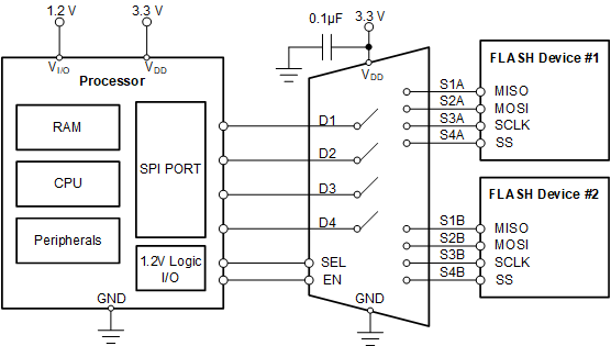
 Application Example
 Block Diagram