SCDS397B November 2018 – August 2025 TMUX6136
PRODUCTION DATA
- 1
- 1 Features
- 2 Applications
- 3 Description
- 4 Pin Configuration and Functions
-
5 Specifications
- 5.1 Absolute Maximum Ratings
- 5.2 ESD Ratings
- 5.3 Thermal Information
- 5.4 Recommended Operating Conditions
- 5.5 Electrical Characteristics (Dual Supplies: ±15V)
- 5.6 Switching Characteristics (Dual Supplies: ±15V)
- 5.7 Electrical Characteristics (Single Supply: 12V)
- 5.8 Switching Characteristics (Single Supply: 12V)
- 5.9 Typical Characteristics
- 6 Detailed Description
- 7 Application and Implementation
- 8 Power Supply Recommendations
- 9 Layout
- 10Device and Documentation Support
- 11Revision History
- 12Mechanical, Packaging, and Orderable Information
Package Options
Mechanical Data (Package|Pins)
- PW|16
Thermal pad, mechanical data (Package|Pins)
Orderable Information
7.2 Typical Application
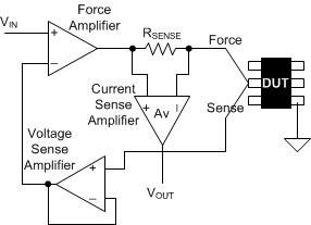
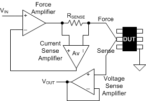
One example of the TMUX6136 precision performance to take advantage of is the implementation of parametric measurement unit (PMU) in the semiconductor automatic test equipment (ATE) application. The PMU is frequently used to characterize and measure the digital pin’s DC characteristics of a device under test (DUT). Among all the PMU’s capabilities, force voltage measure current (FVMC) and force current measure voltage (FCMV) are the two most typical configurations in DC characterizations.
 Figure 7-1 FVMC Measurement in
PMU
 Figure 7-2 FCMV Measurement in
PMU
Figure 7-2 FCMV Measurement in
PMUFigure 7-1 shows a simplified diagram of the PMU in FVMC configuration. The control loop consists of the force amplifier with the voltage sense amplifier (unity gain in this example) making up the feedback path. Current flowing through the DUT is measured by sensing the current flowing through a sense resistor (RSENSE) in series with the DUT. The current sense amplifier with a gain of Av generates a voltage (VOUT) at its output and the voltage can then be measured by an ADC. The voltage produced at the DUT pin stays at the input voltage level (IN) as long as the force amplifier does not rail out (for example, IDUT × RSENSE x Av stays within the input voltage range of the force amplifier). Depending on the level of the DUT current to be measured, different gain settings need to be configured for the current sense amplifier.
Figure 7-2 shows a simplified diagram of the PMU in FCMV mode. The voltage VIN is now converted to a current through the following relationship:
The control loop consists of the force amplifier with the current sense amplifier making up the feedback path. The voltage at the DUT is sensed across the voltage sense amplifier (unity gain in this example) and presented at the output for sample.