SCDS417B March 2022 – December 2023 TMUX7236
PRODUCTION DATA
- 1
- 1 Features
- 2 Applications
- 3 Description
- 4 Pin Configuration and Functions
-
5 Specifications
- 5.1 Absolute Maximum Ratings
- 5.2 ESD Ratings
- 5.3 Thermal Information
- 5.4 Recommended Operating Conditions
- 5.5 Source or Drain Continuous Current
- 5.6 ±15 V Dual Supply: Electrical Characteristics
- 5.7 ±15 V Dual Supply: Switching Characteristics
- 5.8 ±20 V Dual Supply: Electrical Characteristics
- 5.9 ±20 V Dual Supply: Switching Characteristics
- 5.10 44 V Single Supply: Electrical Characteristics
- 5.11 44 V Single Supply: Switching Characteristics
- 5.12 12 V Single Supply: Electrical Characteristics
- 5.13 12 V Single Supply: Switching Characteristics
- 5.14 Typical Characteristics
-
6 Parameter Measurement Information
- 6.1 On-Resistance
- 6.2 Off-Leakage Current
- 6.3 On-Leakage Current
- 6.4 Transition Time
- 6.5 tON(EN) and tOFF(EN)
- 6.6 Break-Before-Make
- 6.7 tON (VDD) Time
- 6.8 Propagation Delay
- 6.9 Charge Injection
- 6.10 Off Isolation
- 6.11 Crosstalk
- 6.12 Bandwidth
- 6.13 THD + Noise
- 6.14 Power Supply Rejection Ratio (PSRR)
- 7 Detailed Description
- 8 Application and Implementation
- 9 Device and Documentation Support
- 10Revision History
- 11Mechanical, Packaging, and Orderable Information
Package Options
Refer to the PDF data sheet for device specific package drawings
Mechanical Data (Package|Pins)
- PW|16
- RUM|16
Thermal pad, mechanical data (Package|Pins)
- RUM|16
Orderable Information
3 Description
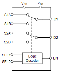
The TMUX7236 is a complementary metal-oxide semiconductor (CMOS) switch with latch-up immunity in a dual channel, 2:1 configuration. The device works well with dual supplies (±5 V to ±22 V), a single supply (5 V to 44 V), or asymmetric supplies (such as VDD = 12 V, VSS = –5 V). The TMUX7236 supports bidirectional analog and digital signals on the source (Sx) and drain (D) pins ranging from VSS to VDD.
All logic control inputs support logic levels from 1.8 V to VDD, allowing for both TTL and CMOS logic compatibility when operating in the valid supply voltage range. Fail-Safe Logic circuitry allows voltages on the control pins to be applied before the supply pin, protecting the device from potential damage.
The TMUX72xx family provides latch-up immunity, preventing undesirable high current events between parasitic structures within the device typically caused by overvoltage events. A latch-up condition typically continues until the power supply rails are turned off and can lead to device failure. The latch-up immunity feature allows the TMUX72xx family of switches and multiplexers to be used in harsh environments.
| PART NUMBER | PACKAGE(1) | PACKAGE SIZE(2) |
|---|---|---|
| TMUX7236 | RUM (WQFN, 16) | 4 mm × 4 mm |
| PW (TSSOP, 16) | 5 mm × 6.4 mm |
 Block Diagram