SLVSER6B May 2020 – November 2020 TPS23730
PRODUCTION DATA
- 1 Features
- 2 Applications
- 3 Description
- 4 Revision History
- 5 Device Comparison Table
- 6 Pin Configuration and Functions
- 7 Specifications
-
8 Detailed Description
- 8.1 Overview
- 8.2 Functional Block Diagram
- 8.3
Feature Description
- 8.3.1 CLSA, CLSB Classification
- 8.3.2 DEN Detection and Enable
- 8.3.3 APD Auxiliary Power Detect
- 8.3.4 PPD Power Detect
- 8.3.5 Internal Pass MOSFET
- 8.3.6 TPH, TPL and BT PSE Type Indicators
- 8.3.7
DC-DC Controller Features
- 8.3.7.1 VCC, VB, VBG and Advanced PWM Startup
- 28
- 8.3.7.2 CS, Current Slope Compensation and Blanking
- 8.3.7.3 COMP, FB, EA_DIS, CP, PSRS and Opto-less Feedback
- 8.3.7.4 FRS Frequency Setting and Synchronization
- 8.3.7.5 DTHR and Frequency Dithering for Spread Spectrum Applications
- 8.3.7.6 SST and Soft-Start of the Switcher
- 8.3.7.7 SST, I_STP, LINEUV and Soft-Stop of the Switcher
- 8.3.8 Switching FET Driver - GATE, GTA2, DT
- 8.3.9 EMPS and Automatic MPS
- 8.3.10 VDD Supply Voltage
- 8.3.11 RTN, AGND, GND
- 8.3.12 VSS
- 8.3.13 Exposed Thermal pads - PAD_G and PAD_S
- 8.4
Device Functional Modes
- 8.4.1 PoE Overview
- 8.4.2 Threshold Voltages
- 8.4.3 PoE Start-Up Sequence
- 8.4.4 Detection
- 8.4.5 Hardware Classification
- 8.4.6 Maintain Power Signature (MPS)
- 8.4.7 Advanced Start-Up and Converter Operation
- 8.4.8 Line Undervoltage Protection and Converter Operation
- 8.4.9 PD Self-Protection
- 8.4.10 Thermal Shutdown - DC-DC Controller
- 8.4.11 Adapter ORing
-
9 Application and Implementation
- 9.1 Application Information
- 9.2
Typical Application
- 9.2.1
Design Requirements
- 9.2.1.1
Detailed Design Procedure
- 9.2.1.1.1 Input Bridges and Schottky Diodes
- 9.2.1.1.2 Input TVS Protection
- 9.2.1.1.3 Input Bypass Capacitor
- 9.2.1.1.4 Detection Resistor, RDEN
- 9.2.1.1.5 Classification Resistor, RCLSA and RCLSB.
- 9.2.1.1.6 Dead Time Resistor, RDT
- 9.2.1.1.7 APD Pin Divider Network, RAPD1, RAPD2
- 9.2.1.1.8 PPD Pin Divider Network, RPPD1, RPPD2
- 9.2.1.1.9 Setting Frequency (RFRS) and Synchronization
- 9.2.1.1.10 Bias Supply Requirements and CVCC
- 9.2.1.1.11 TPH, TPL, and BT Interface
- 9.2.1.1.12 Secondary Soft Start
- 9.2.1.1.13 Frequency Dithering for Conducted Emissions Control
- 9.2.1.1
Detailed Design Procedure
- 9.2.1
Design Requirements
- 10Power Supply Recommendations
- 11Layout
- 12Device and Documentation Support
- 13Mechanical, Packaging, and Orderable Information
Package Options
Mechanical Data (Package|Pins)
- RMT|45
Thermal pad, mechanical data (Package|Pins)
Orderable Information
9.2.1.1.12 Secondary Soft Start
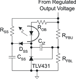
Converters require a soft start on the voltage error amplifier to prevent output overshoot on start-up. Figure 9-2 shows a common implementation of a secondary-side soft start that works with the typical TLV431 error amplifier. The soft-start components consist of DSS, RSS, and CSS. They serve to control the output rate-of-rise by pulling VCOMP down as CSS charges through ROB, the optocoupler, and DSS. This has the added advantage that the TLV431 output and CIZ are preset to the proper value as the output voltage reaches the regulated value, preventing voltage overshoot due to the error amplifier recovery. The secondary-side error amplifier will not become active until there is sufficient voltage on the secondary. The TPS23730 provides an adjustable primary-side soft start, which persists long enough for secondary side voltage-loop soft start to take over. The primary-side current-loop soft start controls the switching MOSFET peak current by applying a slowly rising ramp voltage to a second PWM control input. The PWM is controlled by the lower of the soft-start ramp or the COMP-derived current demand. The actual output voltage rise time is usually much shorter than the internal soft-start period. Initially the primary soft-start ramp limits the maximum current demand as a function of time. Either the current limit, secondary-side soft start, or output regulation assume control of the PWM before the primary soft-start period is over. Since the VCC startup source stays on longer after converter's output voltage is ramped up (VCC startup turns off only when 2.1 V is reached on the SS pin), a large bias winding hold up capacitor is not necessary like in some traditional PWM controllers. Instead, this allows for a small 1-µF ceramic capacitor to be used on VCC.
 Figure 9-2 Error Amplifier Soft Start