SLVSER6B May 2020 – November 2020 TPS23730
PRODUCTION DATA
- 1 Features
- 2 Applications
- 3 Description
- 4 Revision History
- 5 Device Comparison Table
- 6 Pin Configuration and Functions
- 7 Specifications
-
8 Detailed Description
- 8.1 Overview
- 8.2 Functional Block Diagram
- 8.3
Feature Description
- 8.3.1 CLSA, CLSB Classification
- 8.3.2 DEN Detection and Enable
- 8.3.3 APD Auxiliary Power Detect
- 8.3.4 PPD Power Detect
- 8.3.5 Internal Pass MOSFET
- 8.3.6 TPH, TPL and BT PSE Type Indicators
- 8.3.7
DC-DC Controller Features
- 8.3.7.1 VCC, VB, VBG and Advanced PWM Startup
- 28
- 8.3.7.2 CS, Current Slope Compensation and Blanking
- 8.3.7.3 COMP, FB, EA_DIS, CP, PSRS and Opto-less Feedback
- 8.3.7.4 FRS Frequency Setting and Synchronization
- 8.3.7.5 DTHR and Frequency Dithering for Spread Spectrum Applications
- 8.3.7.6 SST and Soft-Start of the Switcher
- 8.3.7.7 SST, I_STP, LINEUV and Soft-Stop of the Switcher
- 8.3.8 Switching FET Driver - GATE, GTA2, DT
- 8.3.9 EMPS and Automatic MPS
- 8.3.10 VDD Supply Voltage
- 8.3.11 RTN, AGND, GND
- 8.3.12 VSS
- 8.3.13 Exposed Thermal pads - PAD_G and PAD_S
- 8.4
Device Functional Modes
- 8.4.1 PoE Overview
- 8.4.2 Threshold Voltages
- 8.4.3 PoE Start-Up Sequence
- 8.4.4 Detection
- 8.4.5 Hardware Classification
- 8.4.6 Maintain Power Signature (MPS)
- 8.4.7 Advanced Start-Up and Converter Operation
- 8.4.8 Line Undervoltage Protection and Converter Operation
- 8.4.9 PD Self-Protection
- 8.4.10 Thermal Shutdown - DC-DC Controller
- 8.4.11 Adapter ORing
-
9 Application and Implementation
- 9.1 Application Information
- 9.2
Typical Application
- 9.2.1
Design Requirements
- 9.2.1.1
Detailed Design Procedure
- 9.2.1.1.1 Input Bridges and Schottky Diodes
- 9.2.1.1.2 Input TVS Protection
- 9.2.1.1.3 Input Bypass Capacitor
- 9.2.1.1.4 Detection Resistor, RDEN
- 9.2.1.1.5 Classification Resistor, RCLSA and RCLSB.
- 9.2.1.1.6 Dead Time Resistor, RDT
- 9.2.1.1.7 APD Pin Divider Network, RAPD1, RAPD2
- 9.2.1.1.8 PPD Pin Divider Network, RPPD1, RPPD2
- 9.2.1.1.9 Setting Frequency (RFRS) and Synchronization
- 9.2.1.1.10 Bias Supply Requirements and CVCC
- 9.2.1.1.11 TPH, TPL, and BT Interface
- 9.2.1.1.12 Secondary Soft Start
- 9.2.1.1.13 Frequency Dithering for Conducted Emissions Control
- 9.2.1.1
Detailed Design Procedure
- 9.2.1
Design Requirements
- 10Power Supply Recommendations
- 11Layout
- 12Device and Documentation Support
- 13Mechanical, Packaging, and Orderable Information
Package Options
Mechanical Data (Package|Pins)
- RMT|45
Thermal pad, mechanical data (Package|Pins)
Orderable Information
8.3.7.2 CS, Current Slope Compensation and Blanking
The current-sense input for the DC-DC converter should be connected to the high side of the current-sense resistor of the switching MOSFET. This voltage drives the current limit comparator and the PWM comparator (see Block Diagram of DC-DC controller). A leading-edge blanking circuit prevents MOSFET turn-on transients from falsely triggering either of these comparators. During the off time, and also during the blanking time that immediately follows, the CS pin is pulled to AGND through an internal pulldown resistor.
The current limit comparator terminates the on-time portion of the switching cycle as soon as VCS exceeds approximately 250 mV (VCSMAX) and the leading edge blanking interval has expired. If the converter is not in current limit, then either the PWM comparator or the maximum duty cycle limiting (DMAX) circuit terminates the on time.
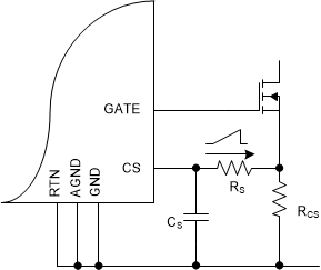
Current-mode control requires addition of a compensation ramp to the sensed inductive (transformer or inductor) current for stability at duty cycles near and over 50%. The TPS23730 provides an internal slope compensation circuit which generates a current that imposes a voltage ramp at the positive input of the PWM comparator to suppress sub-harmonic oscillations. This current flows out of the CS pin. If desired, the magnitude of the slope compensation can be increased by the addition of an external resistor RS (see Figure 8-2) in series with the CS pin. It works with ramp current (IPK = ISL-EX, approximately 20 μA) that flows out of the CS pin when the MOSFET is on. The IPK specification does not include the approximately 2-μA fixed current that flows out of the CS pin.
The TPS23730 has a maximum duty cycle limit of 78%, permitting the design of wide input-range converters with a lower voltage stress on the output rectifiers. While the maximum duty cycle is 78%, converters may be designed that run at duty cycles well below this for a narrower, 36-V to 57-V range.
Most current-mode control papers and application notes define the slope compensation values in terms of VPP/TS (peak ramp voltage / switching period); however, Electrical Characteristics: DC-DC Controller Section specifies the slope peak (VSLOPE) based on the maximum duty cycle. Assuming that the desired slope, VSLOPE-D (in mV/period), is based on the full period, compute RS per Equation 1 where VSLOPE, DMAX, and ISL-EX are from Electrical Characteristics: DC-DC Controller Section with voltages in mV, current in μA, and the duty cycle is unitless (for example, DMAX = 0.78).

 Figure 8-2 Additional Slope Compensation
The TPS23730 blanker timing is precise enough that the traditional R-C filters on CS can be eliminated. This avoids current-sense waveform distortion, which tends to get worse at light output loads. There may be some situations or designers that prefer an R-C approach, for example if the presence of RS causes increased noise, due to adjacent noisy signals, to appear at CS pin. The TPS23730 provides a pulldown on CS (~400 Ω) during the GATE OFF-time to improve sensing when an R-C filter must be used, by reducing cycle-to-cycle carry-over voltage on CS.
Routing between the current-sense resistor and the CS pin should be short to minimize cross-talk from noisy traces such as the gate drive signal and the CP signal.