SLVSER6B May 2020 – November 2020 TPS23730
PRODUCTION DATA
- 1 Features
- 2 Applications
- 3 Description
- 4 Revision History
- 5 Device Comparison Table
- 6 Pin Configuration and Functions
- 7 Specifications
-
8 Detailed Description
- 8.1 Overview
- 8.2 Functional Block Diagram
- 8.3
Feature Description
- 8.3.1 CLSA, CLSB Classification
- 8.3.2 DEN Detection and Enable
- 8.3.3 APD Auxiliary Power Detect
- 8.3.4 PPD Power Detect
- 8.3.5 Internal Pass MOSFET
- 8.3.6 TPH, TPL and BT PSE Type Indicators
- 8.3.7
DC-DC Controller Features
- 8.3.7.1 VCC, VB, VBG and Advanced PWM Startup
- 28
- 8.3.7.2 CS, Current Slope Compensation and Blanking
- 8.3.7.3 COMP, FB, EA_DIS, CP, PSRS and Opto-less Feedback
- 8.3.7.4 FRS Frequency Setting and Synchronization
- 8.3.7.5 DTHR and Frequency Dithering for Spread Spectrum Applications
- 8.3.7.6 SST and Soft-Start of the Switcher
- 8.3.7.7 SST, I_STP, LINEUV and Soft-Stop of the Switcher
- 8.3.8 Switching FET Driver - GATE, GTA2, DT
- 8.3.9 EMPS and Automatic MPS
- 8.3.10 VDD Supply Voltage
- 8.3.11 RTN, AGND, GND
- 8.3.12 VSS
- 8.3.13 Exposed Thermal pads - PAD_G and PAD_S
- 8.4
Device Functional Modes
- 8.4.1 PoE Overview
- 8.4.2 Threshold Voltages
- 8.4.3 PoE Start-Up Sequence
- 8.4.4 Detection
- 8.4.5 Hardware Classification
- 8.4.6 Maintain Power Signature (MPS)
- 8.4.7 Advanced Start-Up and Converter Operation
- 8.4.8 Line Undervoltage Protection and Converter Operation
- 8.4.9 PD Self-Protection
- 8.4.10 Thermal Shutdown - DC-DC Controller
- 8.4.11 Adapter ORing
-
9 Application and Implementation
- 9.1 Application Information
- 9.2
Typical Application
- 9.2.1
Design Requirements
- 9.2.1.1
Detailed Design Procedure
- 9.2.1.1.1 Input Bridges and Schottky Diodes
- 9.2.1.1.2 Input TVS Protection
- 9.2.1.1.3 Input Bypass Capacitor
- 9.2.1.1.4 Detection Resistor, RDEN
- 9.2.1.1.5 Classification Resistor, RCLSA and RCLSB.
- 9.2.1.1.6 Dead Time Resistor, RDT
- 9.2.1.1.7 APD Pin Divider Network, RAPD1, RAPD2
- 9.2.1.1.8 PPD Pin Divider Network, RPPD1, RPPD2
- 9.2.1.1.9 Setting Frequency (RFRS) and Synchronization
- 9.2.1.1.10 Bias Supply Requirements and CVCC
- 9.2.1.1.11 TPH, TPL, and BT Interface
- 9.2.1.1.12 Secondary Soft Start
- 9.2.1.1.13 Frequency Dithering for Conducted Emissions Control
- 9.2.1.1
Detailed Design Procedure
- 9.2.1
Design Requirements
- 10Power Supply Recommendations
- 11Layout
- 12Device and Documentation Support
- 13Mechanical, Packaging, and Orderable Information
Package Options
Mechanical Data (Package|Pins)
- RMT|45
Thermal pad, mechanical data (Package|Pins)
Orderable Information
8.4.7 Advanced Start-Up and Converter Operation
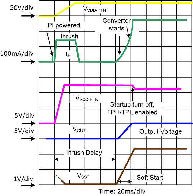
The internal PoE undervoltage lockout (UVLO) circuit holds the hotswap switch off before the PSE provides full voltage to the PD. This prevents the converter circuits from loading the PoE input during detection and classification. The converter circuits discharges CBULK, CVCC, CVB and CVBG while the PD is unpowered. Thus VVDD-RTN will be a small voltage until just after full voltage is applied to the PD, as seen in Figure 8-7.
The PSE drives the PI voltage to the operating range once it has decided to power up the PD. When VVDD rises above the UVLO turnon threshold (VUVLO-R, approximately 37.6 V) with RTN high, the TPS23730 enables the hotswap MOSFET with an approximately 140-mA (inrush) current limit. See the waveforms of Figure 8-9 for an example. Converter switching is disabled while CBULK charges and VRTN falls from VVDD to nearly VVSS; however, the converter start-up circuit is allowed to charge CVCC (the VB regulator also powers the internal converter circuits as VVCC rises). Once the inrush current falls about 10% below the inrush current limit, the PD current limit switches to the operational level (approximately 1.85 A). Additionally, once the inrush period duration has also exceeded approximately 84 ms (end of inrush phase), the converter switching is allowed to start, once VVCC also goes above its UVLO (approximately 8.25 V).
Continuing the start-up sequence shown in Figure 8-9, once VVCC goes above its UVLO , the soft-start (SST) capacitor is first discharged with controlled current (ISSD) below nominally 0.2 V (VSFST) if the discharge was not already completed, then it is gradually recharged until it reaches ~0.25 V (VSSOFS in closed-loop mode) at which point the converter switching is enabled, following the closed loop controlled soft-start sequence. Note that the startup current source capability is such that it can fully maintain VVCC during the converter soft-start without requiring any significant CVCC capacitance, in 48 V input applications. At the end of the soft-start period, more specifically when SST voltage has exceeded ~2 V (VSTUOF), the startup current source is turned off. VVCC falls as it powers the internal circuits including the switching MOSFET gate. If the converter control-bias output rises to support VVCC before it falls to VCUVLO_F (~6.1 V), a successful start-up occurs. Figure 8-9 shows a small droop in VVCC while the output voltage rises smoothly and a successful start-up occurs.
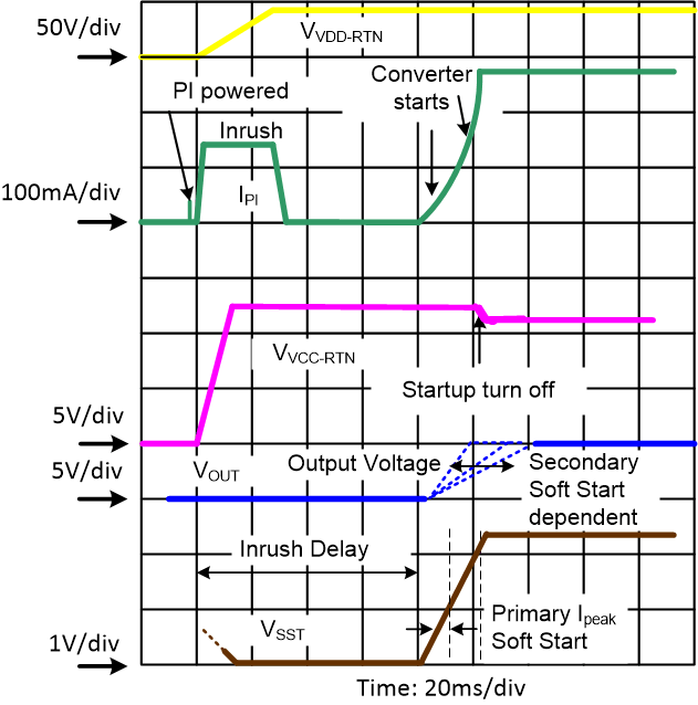
Figure 8-10 also illustrates similar scenario if optocoupler feedback is used instead of PSR. In this case, the converter switching is enabled when VSST exceeds approximately 0.6 V (VSSOFS in peak current mode).
 Figure 8-9 Power Up and Start - Flyback with PSR
 Figure 8-10 Power Up and Start - with Opto Feedback
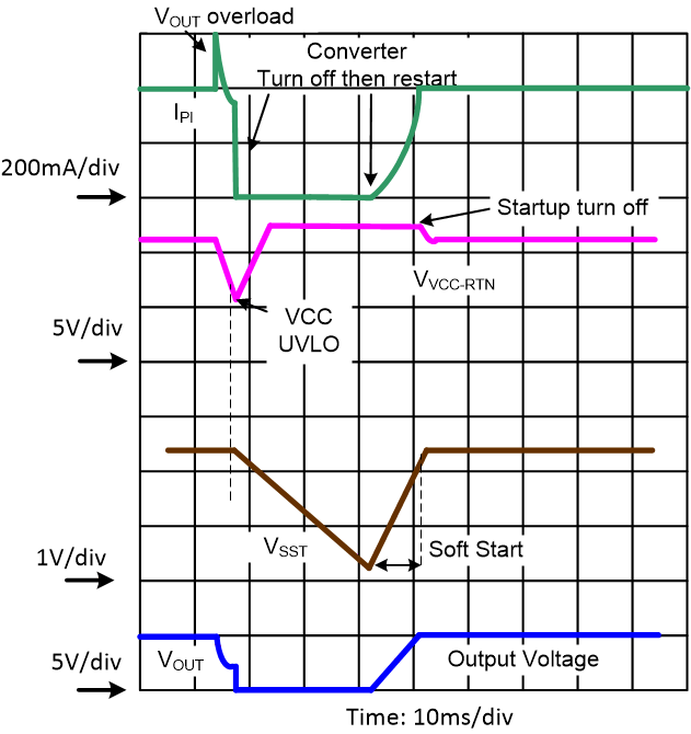
The converter shuts off when VVCC falls below its lower UVLO. This can happen when power is removed from the PD, or during a fault on a converter output rail. When one output is shorted, all the output voltages fall including the one that powers VCC. The control circuit discharges VCC until it hits the lower UVLO and turns off. A restart initiates if the converter turns off and there is sufficient VDD voltage. This type of operation is sometimes referred to as hiccup mode, which when combined with the soft-start provides robust output short protection by providing time-average heating reduction of the output rectifier.
Figure 8-11 illustrates the situation when there is severe overload at the main output which causes VCC hiccup. After VCC went below its UVLO due to the overload, the startup source is turned back on. Then, a new soft-start cycle is reinitiated, the soft-start capacitor being first discharged with controlled current, introducing a short pause before the output voltage is ramped up.
 Figure 8-11 Restart Following Severe Overload at Main Output of PSR Flyback DC-DC Converter
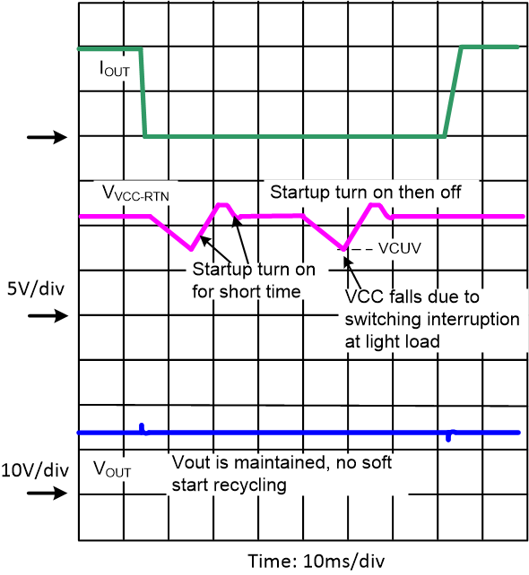
Also, when a VCC fall occurs, the TPS23730 can differentiate between an overload and a light load condition. For example a diode-rectified flyback with optocoupled feedback may have its VCC rail to fall in situation of light load due to temporary switching stop. In this case, the output voltage has to be maintained and a soft-start would not be acceptable. To address this case, if VVCC falls below approximately 7.1 V due to light load, the TPS23730 turns back on the startup immediately and for a short period of time to bring VCC voltage back up, and there is no soft-start recycling.
 Figure 8-12 Startup Operation if VCC Undervoltage is caused by Light Load Condition of Diode-rectified Flyback DC-DC Converter
If VVDD-VSS drops below the lower PoE UVLO (VUVLO_F, approximately 32 V), the hotswap MOSFET is turned off, but the converter still runs (unless LINEUV input is pulled low). The converter stops if VVCC falls below the VCUVLO_F (~6.1 V), the hotswap is in inrush current limit, the SST pin is pulled to ground, or the converter is in thermal shutdown.