SLVSDW2B December 2018 – November 2020 TPS23755
PRODUCTION DATA
- 1 Features
- 2 Applications
- 3 Description
- 4 Revision History
- 5 Pin Configuration and Functions
- 6 Specifications
-
7 Detailed Description
- 7.1 Overview
- 7.2 Functional Block Diagram
- 7.3
Feature Description
- 7.3.1 CLS Classification
- 7.3.2 DEN Detection and Enable
- 7.3.3 Internal Pass MOSFET
- 7.3.4
DC-DC Controller Features
- 7.3.4.1 VCC, VB and Advanced PWM Startup
- 7.3.4.2 CS, Current Slope Compensation and Blanking
- 7.3.4.3 COMP, FB, CP and Opto-less Feedback
- 7.3.4.4 FRS Frequency Setting and Synchronization
- 7.3.4.5 Frequency Dithering for Spread Spectrum Applications
- 7.3.4.6 SST and Soft-Start of the Switcher
- 7.3.4.7 AUX_V, AUX_D and Secondary Adapter Or'ing
- 7.3.5 Internal Switching FET - DRAIN, RSNS, SRF and SRR
- 7.3.6 VPD Supply Voltage
- 7.3.7 VDD Supply Voltage
- 7.3.8 GND
- 7.3.9 VSS
- 7.3.10 Exposed Thermal PAD
- 7.4 Device Functional Modes
-
8 Application and Implementation
- 8.1 Application Information
- 8.2
Typical Application
- 8.2.1 Design Requirements
- 8.2.2
Detailed Design Procedure
- 8.2.2.1 Input Bridges and Schottky Diodes
- 8.2.2.2 Protection, D1
- 8.2.2.3 Capacitor, C1
- 8.2.2.4 Detection Resistor, RDEN
- 8.2.2.5 Classification Resistor, RCLS
- 8.2.2.6 Bulk Capacitance, CBULK
- 8.2.2.7 Output Voltage Feedback Divider, RAUX, R1,R2
- 8.2.2.8 Setting Frequency, RFRS
- 8.2.2.9 Frequency Dithering, RDTR and CDTR
- 8.2.2.10 Bias Voltage, CVB and DVB
- 8.2.2.11 Transformer design, T1
- 8.2.2.12 Current Sense Resistor, RCS
- 8.2.2.13 Current Slope Compensation, RS
- 8.2.2.14 Bias Supply Requirements, CCC, DCC
- 8.2.2.15 Switching Transformer Considerations, RVCC and CCC2
- 8.2.2.16 Primary FET Clamping, RCL, CCL, and DCL
- 8.2.2.17 Converter Output Capacitance, COUT
- 8.2.2.18 Secondary Output Diode Rectifier, DOUT
- 8.2.2.19 Slew rate control, RSRF and RSRR
- 8.2.2.20 Shutdown at Low Temperatures, DVDD and CVDD
- 8.2.3 Application Curves
- 9 Power Supply Recommendations
- 10Layout
- 11Device and Documentation Support
- 12Mechanical, Packaging, and Orderable Information
Package Options
Mechanical Data (Package|Pins)
- RJJ|23
Thermal pad, mechanical data (Package|Pins)
Orderable Information
7.4.1 PoE Overview
The following text is intended as an aid in understanding the operation of the TPS23755, but it is not a substitute for the actual IEEE 802.3at standard. The IEEE 802.3at standard is an update to IEEE 802.3-2008 clause 33 (PoE), adding high-power options and enhanced classification.
Generally speaking, a device compliant to IEEE 802.3-2008 is referred to as a Type 1 device, and devices with high power or enhanced classification is referred to as Type 2 devices. The TPS23755 is intended to power Type 1 devices (up to 13 W), and is fully compliant to IEEE 802.3at for hardware classes 0 - 3. Standards change and must always be referenced when making design decisions.
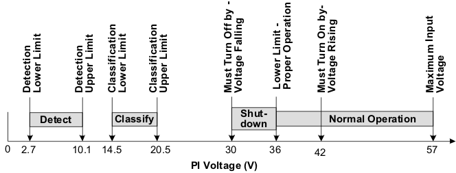
The IEEE 802.3at standard defines a method of safely powering a PD (powered device) over a cable, and then removing power if a PD is disconnected. The process proceeds through an idle state and three operational states of detection, classification, and operation. The PSE leaves the cable unpowered (idle state) while it periodically looks to see if something has been plugged in; this is referred to as detection. The low power levels used during detection are unlikely to damage devices not designed for PoE. If a valid PD signature is present, the PSE may inquire how much power the PD requires; this is referred to as (hardware) classification. Only Type 2 PSEs are required to do hardware classification. The PD may return the default 13-W current-encoded class, or one of four other choices. The PSE may then power the PD if it has adequate capacity. Once started, the PD must present the maintain power signature (MPS) to assure the PSE that it is still present. The PSE monitors its output for a valid MPS, and turns the port off if it loses the MPS. Loss of the MPS returns the PSE to the idle state. Figure 7-5 shows the operational states as a function of PD input voltage.
 Figure 7-5 Operational States
The PD input is typically an RJ-45 eight-lead connector which is referred to as the power interface (PI). PD input requirements differ from PSE output requirements to account for voltage drops in the cable and operating margin. The IEEE 802.3at standard uses a cable resistance of 20 Ω for Type 1 devices to derive the voltage limits at the PD based on the PSE output voltage requirements. Although the standard specifies an output power of 15.4 W at the PSE, only 13 W is available at the PI due to the worst-case power loss in the cable. The PSE can apply voltage either between the RX and TX pairs (pins 1–2 and 3–6 for 10baseT or 100baseT), or between the two spare pairs (4–5 and 7–8). Power application to the same pin combinations in 1000baseT systems is recognized in IEEE 802.3at. 1000baseT systems can handle data on all pairs, eliminating the spare pair terminology. The PSE may only apply voltage to one set of pairs at a time. The PD uses input diode bridges to accept power from any of the possible PSE configurations. The voltage drops associated with the input bridges create a difference between the standard limits at the PI and the TPS23755 specifications.
The PSE is permitted to disconnect a PD if it draws more than its maximum class power over a one second interval. A Type 1 PSE compliant to IEEE 802.3at is required to limit current to between 400 mA and 450 mA during powered operation, and it must disconnect the PD if it draws this current for more than 75 ms. Class 0 and 3 PDs may draw up to 400-mA peak currents for up to 50 ms. The PSE may set lower output current limits based on the declared power requirements of the PD.