SLVSFC9B October 2020 – March 2022 TPS25947
PRODUCTION DATA
- 1 Features
- 2 Applications
- 3 Description
- 4 Revision History
- 5 Device Comparison Table
- 6 Pin Configuration and Functions
- 7 Specifications
-
8 Detailed Description
- 8.1 Overview
- 8.2 Functional Block Diagram
- 8.3
Feature Description
- 8.3.1 Input Reverse Polarity Protection
- 8.3.2 Undervoltage Lockout (UVLO and UVP)
- 8.3.3 Overvoltage Lockout (OVLO)
- 8.3.4 Overvoltage Clamp (OVC)
- 8.3.5 Inrush Current, Overcurrent, and Short Circuit Protection
- 8.3.6 Analog Load Current Monitor
- 8.3.7 Reverse Current Protection
- 8.3.8 Overtemperature Protection (OTP)
- 8.3.9 Fault Response and Indication (FLT)
- 8.3.10 Auxiliary Channel Control (AUXOFF)
- 8.3.11 Power Good Indication (PG)
- 8.4 Device Functional Modes
- 9 Application and Implementation
- 10Power Supply Recommendations
- 11Layout
- 12Device and Documentation Support
- 13Mechanical, Packaging, and Orderable Information
Package Options
Mechanical Data (Package|Pins)
- RPW|10
Thermal pad, mechanical data (Package|Pins)
Orderable Information
9.3.2.3 Setting Output Voltage Rise Time (tR)
For a successful design, the junction
temperature of device must be kept below the absolute maximum rating during both dynamic
(start-up) and steady-state conditions. Dynamic power stresses often are an order of
magnitude greater than the static stresses, so it is important to determine the right
start-up time and inrush current limit required with system capacitance to avoid thermal
shutdown during start-up.
The slew rate (SR) needed to achieve the desired output rise time can be calculated as:
Equation 12. 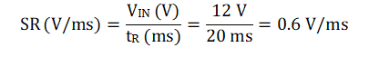
The CdVdt needed to achieve this slew rate can be calculated as:
Equation 13. 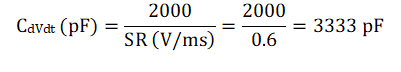
Choose the nearest standard capacitor value as 3300 pF.
For this slew rate, the inrush current can be calculated as:
Equation 14. 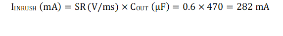
The average power dissipation inside the part during inrush can be calculated as:
Equation 15. 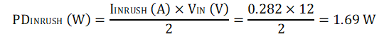
For the given
power dissipation, the thermal shutdown time of the device must be greater than the
ramp-up time tR to avoid start-up failure. Figure 9-3 shows the thermal
shutdown limit, for 1.69 W of power, the shutdown time is more than 10 s which is very
large as compared to tR = 20 ms. Therefore, it is safe to use 20 ms as the
startup time for this application.
Figure 9-3 Thermal Shut-Down Plot During
Inrush