SLVSBV5C June 2014 – September 2021 TPS55340-Q1
PRODUCTION DATA
- 1 Features
- 2 Applications
- 3 Description
- 4 Revision History
- 5 Pin Configuration and Functions
- 6 Specifications
-
7 Detailed Description
- 7.1 Overview
- 7.2 Functional Block Diagram
- 7.3 Feature Description
- 7.4 Device Functional Modes
-
8 Application and Implementation
- 8.1 Application Information
- 8.2
Typical Applications
- 8.2.1
TPS55340-Q1 Boost Converter
- 8.2.1.1 Design Requirements
- 8.2.1.2
Detailed Design Procedure
- 8.2.1.2.1 Custom Design With WEBENCH® Tools
- 8.2.1.2.2 Selecting the Switching Frequency (R4)
- 8.2.1.2.3 Determining the Duty Cycle
- 8.2.1.2.4 Selecting the Inductor (L1)
- 8.2.1.2.5 Computing the Maximum Output Current
- 8.2.1.2.6 Selecting the Output Capacitor (C8 through C10)
- 8.2.1.2.7 Selecting the Input Capacitors (C2 and C7)
- 8.2.1.2.8 Setting the Output Voltage (R1 and R2)
- 8.2.1.2.9 Setting the Soft-Start Time (C7)
- 8.2.1.2.10 Selecting the Schottky Diode (D1)
- 8.2.1.2.11 Compensating the Control Loop (R3, C4, and C5)
- 8.2.1.3 Application Curves
- 8.2.2
TPS55340-Q1 SEPIC Converter
- 8.2.2.1 Design Requirements
- 8.2.2.2
Detailed Design Procedure
- 8.2.2.2.1 Selecting the Switching Frequency (R4)
- 8.2.2.2.2 Duty Cycle
- 8.2.2.2.3 Selecting the Inductor (L1)
- 8.2.2.2.4 Calculating the Maximum Output Current
- 8.2.2.2.5 Selecting the Output Capacitor (C8 Through C10)
- 8.2.2.2.6 Selecting the Series Capacitor (C6)
- 8.2.2.2.7 Selecting the Input Capacitor (C2 and C7)
- 8.2.2.2.8 Selecting the Schottky Diode (D1)
- 8.2.2.2.9 Setting the Output Voltage (R1 and R2)
- 8.2.2.2.10 Setting the Soft-Start Time (C3)
- 8.2.2.2.11 Mosfet Rating Considerations
- 8.2.2.2.12 Compensating the Control Loop (R3 and C4)
- 8.2.2.3 Application Curves
- 8.2.1
TPS55340-Q1 Boost Converter
- 9 Power Supply Recommendations
- 10Layout
- 11Device and Documentation Support
- 12Mechanical, Packaging, and Orderable Information
Package Options
Mechanical Data (Package|Pins)
- RTE|16
Thermal pad, mechanical data (Package|Pins)
- RTE|16
Orderable Information
8.2.1.2.3 Determining the Duty Cycle
The input-to-output voltage-conversion ratio of the TPS55340-Q1 device is limited by the worst-case maximum duty cycle of 89% and the minimum duty cycle, which is determined by the minimum on time of 77 ns and the switching frequency. Use Equation 9 to calculate the minimum duty cycle. Selecting a 600-kHz switching frequency, the minimum duty cycle is calculated as 4%.
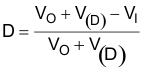
The duty cycle at which the converter operates is dependent on the mode in which the converter is running. If the converter is running in Discontinuous conduction mode (DCM) where the inductor current ramps to zero at the end of each cycle, the duty cycle varies with changes of the load much more than when running in Continuous conduction mode (CCM). In Continuous conduction mode where the inductor maintains a minimum DC current, the duty cycle is related primarily to the input and output voltages as calculated with Equation 10. Assume a 0.5-V drop (V(D)) across the Schottky rectifier. At the minimum input of 5 V, the duty cycle is 80%. At the maximum input of 12 V, the duty cycle is 51%.
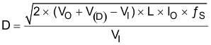
At light loads, the converter operates in DCM. In this case, the duty cycle is a function of the following, as calculated in Equation 11:
- Load
- Input voltage
- Output voltages
- Inductance
- Switching frequency
The light-load duty cycle can be calculated only after an inductance is selected (see Section 8.2.1.2.4). While operating in DCM with very-light load conditions, the duty cycle demand forces the TPS55340-Q1 device to operate with the minimum on time. The converter then begins pulse skipping, which can increase the output ripple.
All converters using a diode as the freewheeling or catch component have a load-current level at which the converters transition from DCM to CCM. The transit from DCM to CCM is the point when the inductor current falls to zero during the off time of the power switch. At higher load currents, the inductor current does not fall to zero and the diode and switch current assume a trapezoidal wave-shape as opposed to a triangular wave-shape. The load current boundary between discontinuous conduction and continuous conduction is calculated for a set of converter parameters as shown in Equation 12.
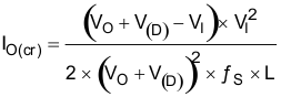
where
- VO is the output voltage of the converter in volts (V).
- V(D) is the forward conduction voltage drop across the rectifier or catch diode in volts (V).
- VI is the input voltage to the converter in volts (V).
- IO is the output current of the converter in amperes (A).
- L is the inductor value in henries (H).
- ƒS is the switching frequency in hertz (Hz).
For loads higher than the result of the Equation 12, the duty cycle is given by Equation 10. For loads less than the results of Equation 12, the duty cycle is given Equation 11.
Unless otherwise stated, the design equations that follow assume that the converter is running in Continuous conduction mode, which typically results in a higher efficiency for the power levels of this converter.