SLVSAX2B September   2011  – June 2020 TPS61170-Q1

PRODUCTION DATA.  

  1. Features
  2. Applications
  3. Description
    1.     Device Images
      1.      Typical Application
  4. Revision History
  5. Pin Configuration and Functions
    1.     Pin Functions
  6. Specifications
    1. 6.1 Absolute Maximum Ratings
    2. 6.2 ESD Ratings
    3. 6.3 Recommended Operating Conditions
    4. 6.4 Thermal Information
    5. 6.5 Electrical Characteristics
    6. 6.6 Switching Characteristics
    7. 6.7 Typical Characteristics
  7. Detailed Description
    1. 7.1 Overview
    2. 7.2 Functional Block Diagram
    3. 7.3 Feature Description
      1. 7.3.1 Soft Start-up
      2. 7.3.2 Overcurrent Protection
      3. 7.3.3 Undervoltage Lockout
      4. 7.3.4 Thermal Shutdown
      5. 7.3.5 Enable and Shutdown
    4. 7.4 Device Functional Modes
      1. 7.4.1 PWM Program Mode
      2. 7.4.2 1-Wire Program Mode
      3. 7.4.3 EasyScale
    5. 7.5 Programming
      1. 7.5.1 Feedback Reference Program Mode Selection
  8. Application and Implementation
    1. 8.1 Application Information
    2. 8.2 Typical Applications
      1. 8.2.1 12-V to 24-V DC-DC Power Conversion
        1. 8.2.1.1 Design Requirements
        2. 8.2.1.2 Detailed Design Procedure
          1. 8.2.1.2.1 Program Output Voltage
          2. 8.2.1.2.2 Maximum Output Current
          3. 8.2.1.2.3 Switch Duty Cycle
          4. 8.2.1.2.4 Inductor Selection
          5. 8.2.1.2.5 Schottky Diode Selection
          6. 8.2.1.2.6 Compensation Capacitor Selection
          7. 8.2.1.2.7 Input and Output Capacitor Selection
        3. 8.2.1.3 Application Curve
      2. 8.2.2 5-V to 12-V DC-DC Power Conversion With Programmable Feedback Reference Voltage
      3. 8.2.3 12-V SEPIC (Buck-Boost) Converter
  9. Power Supply Recommendations
  10. 10Layout
    1. 10.1 Layout Guidelines
    2. 10.2 Layout Example
    3. 10.3 Thermal Considerations
  11. 11Device and Documentation Support
    1. 11.1 Device Support
      1. 11.1.1 Third-Party Products Disclaimer
    2. 11.2 Documentation Support
      1. 11.2.1 Related Documentation
    3. 11.3 Support Resources
    4. 11.4 Trademarks
    5. 11.5 Electrostatic Discharge Caution
    6. 11.6 Glossary
  12. 12Mechanical, Packaging, and Orderable Information

Package Options

Mechanical Data (Package|Pins)
Thermal pad, mechanical data (Package|Pins)
Orderable Information

Program Output Voltage

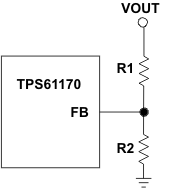
TPS61170-Q1 pro_vo_lvs789.gifFigure 16. Program Output Voltage

To program the output voltage, select the values of R1 and R2 (see Figure 16) according to Equation 2.

Equation 2. TPS61170-Q1 q_vout_lvs789.gif

Considering the leakage current through the resistor divider and noise decoupling to FB pin, an optimum value for R2 is approximately 10 k. The output voltage tolerance depends on the accuracy of the reference voltage and the tolerance of R1 and R2.