SLVSHJ8 February   2024 TPS61299-Q1

PRODUCTION DATA  

  1.   1
  2. Features
  3. Applications
  4. Description
  5. Pin Configuration and Functions
  6. Specifications
    1. 5.1 Absolute Maximum Ratings
    2. 5.2 ESD Ratings
    3. 5.3 Recommended Operating Conditions
    4. 5.4 Thermal Information
    5. 5.5 Electrical Characteristics
    6. 5.6 Typical Characteristics
  7. Detailed Description
    1. 6.1 Overview
    2. 6.2 Functional Block Diagram
    3. 6.3 Feature Description
      1. 6.3.1  Boost Control Operation
      2. 6.3.2  Version Detection
      3. 6.3.3  Under-voltage Lockout
      4. 6.3.4  Switching Frequency
      5. 6.3.5  Input Current Limit
      6. 6.3.6  Enable and Disable
      7. 6.3.7  Soft-Start Timing
      8. 6.3.8  Down Mode
      9. 6.3.9  Pass-Through Operation
      10. 6.3.10 Output Short-to-Ground Protection
      11. 6.3.11 Thermal Shutdown
    4. 6.4 Device Functional Modes
      1. 6.4.1 Fast Load Transient Mode and Normal Mode
  8. Application and Implementation
    1. 7.1 Application Information
    2. 7.2 Typical Application-Li-ion Battery to 5V Boost Converter Under Fast Mode
      1. 7.2.1 Design Requirements
      2. 7.2.2 Detailed Design Procedure
        1. 7.2.2.1 Maximum Output Current
        2. 7.2.2.2 Inductor Selection
        3. 7.2.2.3 Output Capacitor Selection
        4. 7.2.2.4 Input Capacitor Selection
      3. 7.2.3 Application Curves
    3. 7.3 Typical Application-Li-ion Battery to 5V Boost Converter Under Normal Mode
      1. 7.3.1 Design Requirements
      2. 7.3.2 Application Curves
    4. 7.4 Power Supply Recommendations
    5. 7.5 Layout
      1. 7.5.1 Layout Guidelines
      2. 7.5.2 Layout Example
      3. 7.5.3 Thermal Information
  9. Device and Documentation Support
    1. 8.1 Device Support
      1. 8.1.1 Third-Party Products Disclaimer
    2. 8.2 Documentation Support
      1. 8.2.1 Related Documentation
    3. 8.3 Receiving Notification of Documentation Updates
    4. 8.4 Support Resources
    5. 8.5 Trademarks
    6. 8.6 Electrostatic Discharge Caution
    7. 8.7 Glossary
  10. Revision History
  11. 10Mechanical, Packaging, and Orderable Information

Package Options

Mechanical Data (Package|Pins)
Thermal pad, mechanical data (Package|Pins)
Orderable Information

Thermal Information

The maximum junction temperature is restricted to 125°C under normal operating conditions. Calculate the maximum allowable dissipation, PD(max), and maintain the actual power dissipation less than or equal to PD(max). The maximum-power-dissipation limit is determined using Equation 5.
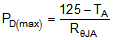
Equation 5. GUID-7926ED7C-E052-43DA-BE15-706E39DDBC90-low.gif

where

  • TA is the maximum ambient temperature for the application
  • ƟJA is the junction-to-ambient thermal resistance given in the Thermal Information table.

The TPS61299-Q1 comes in a WCSP or SOT583 package. The real junction-to-ambient thermal resistance of the package greatly depends on the PCB type and layout. Using thick PCB copper and soldering GND pin to a large ground plate enhances the thermal performance. Using more vias connects the ground plate on the top layer and bottom layer around the IC without solder mask also improves the thermal capability.