SLVSCD6A December   2015  – January 2021 TPS62097

PRODUCTION DATA  

  1. Features
  2. Applications
  3. Description
  4. Revision History
  5. Device Options
  6. Pin Configuration and Functions
  7. Specifications
    1. 7.1 Absolute Maximum Ratings
    2. 7.2 ESD Ratings
    3. 7.3 Recommend Operating Conditions
    4. 7.4 Thermal Information
    5. 7.5 Electrical Characteristics
    6. 7.6 Typical Characteristics
  8. Detailed Description
    1. 8.1 Overview
    2. 8.2 Functional Block Diagram
    3. 8.3 Feature Description
      1. 8.3.1 100% Duty Cycle Mode
      2. 8.3.2 Switch Current Limit and Hiccup Short Circuit Protection
      3. 8.3.3 Undervoltage Lockout (UVLO)
      4. 8.3.4 Thermal Shutdown
    4. 8.4 Device Function Modes
      1. 8.4.1 Enable and Disable (EN)
      2. 8.4.2 Power Save Mode and Forced PWM Mode (MODE)
      3. 8.4.3 Soft Start-up (SS/TR)
      4. 8.4.4 Voltage Tracking (SS/TR)
      5. 8.4.5 Power Good (PG)
  9. Application and Implementation
    1. 9.1 Application Information
    2. 9.2 1.2-V Output Application
      1. 9.2.1 Design Requirements
      2. 9.2.2 Detailed Design Procedure
        1. 9.2.2.1 Setting the Output Voltage
        2. 9.2.2.2 Output Filter Design
        3. 9.2.2.3 Inductor Selection
        4. 9.2.2.4 Capacitor Selection
      3. 9.2.3 Application Performance Curves
      4. 9.2.4 Coincidental Voltage Tracking
        1. 9.2.4.1 Design Requirements
        2. 9.2.4.2 Detailed Design Procedure
        3. 9.2.4.3 Application Performance Curve
      5. 9.2.5 Switching Frequency Selection
        1. 9.2.5.1 Design Requirements
        2. 9.2.5.2 Detailed Design Procedure
        3. 9.2.5.3 Application Performance Curves
  10. 10Power Supply Recommendations
  11. 11Layout
    1. 11.1 Layout Guidelines
    2. 11.2 Layout Example
      1. 11.2.1 Thermal Information
  12. 12Device and Documentation Support
    1. 12.1 Device Support
      1. 12.1.1 Third-Party Products Disclaimer
    2. 12.2 Support Resources
    3. 12.3 Receiving Notification of Documentation Updates
    4. 12.4 Trademarks
    5. 12.5 Electrostatic Discharge Caution
    6. 12.6 Glossary
  13. 13Mechanical, Packaging, and Orderable Information

Package Options

Mechanical Data (Package|Pins)
Thermal pad, mechanical data (Package|Pins)
Orderable Information

Application Performance Curves

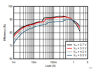
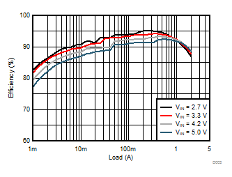
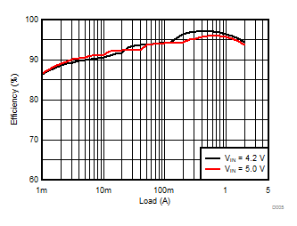
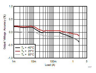
TA = 25°C, VIN = 3.6 V, unless otherwise noted.
GUID-AA32AC17-9D9B-4040-9249-481AADBE8074-low.gif
VOUT = 1.2 V
Figure 9-2 Efficiency, PWM/PSM Mode (2.0 MHz)
GUID-72A8D68D-7C22-4459-994B-E71021DCB8C9-low.gif
VOUT = 1.8 V
Figure 9-4 Efficiency, PWM/PSM Mode (2.0 MHz)
GUID-58247D09-9994-409A-945C-91EE724F085D-low.gif
VOUT = 3.3 V
Figure 9-6 Efficiency, PWM/PSM Mode (2.0 MHz)
GUID-CBEEC360-C260-4DAF-8CDE-05DC469A1C22-low.gif
VOUT = 1.2 V
Figure 9-8 Load Regulation, PWM/PSM Mode (2.0 MHz)
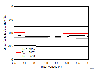
GUID-11AA85D4-3677-4885-AED2-4BE797EB5A19-low.gif
VOUT = 1.2 V IOUT = 500 mA
Figure 9-10 Line Regulation, Forced PWM Mode (2.0 MHz)
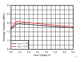
GUID-A59705E4-F184-4F49-AF2C-E863EDAB7915-low.gif
VOUT = 1.2 V MODE = High after PWM/PSM Selection
Figure 9-12 Switching Frequency, Forced PWM Mode (2.0 MHz)
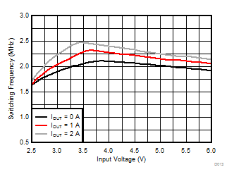
GUID-72251680-0D52-4E62-9C75-6103CCD02556-low.gif
VOUT = 1.2 V MODE = Open
Figure 9-14 Switching Frequency, Forced PWM Mode (2.5 MHz)
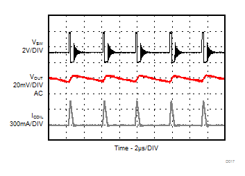
GUID-BBC591FC-7401-4864-934E-5CDCB4FA8EB9-low.gif
VOUT = 1.2 V IOUT = 30 mA
Figure 9-16 Output Ripple, Power Save Operation
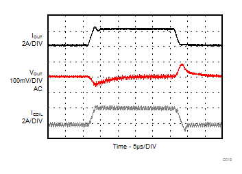
GUID-BEC6E5D8-1D35-458F-B19A-D13CD51DAA75-low.gif
VOUT = 1.2 V IOUT = 0 A to 2 A, 1 A / µs
Figure 9-18 Load Transient, Forced PWM Mode (2.0 MHz)
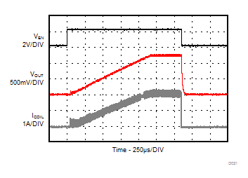
GUID-621AEB9D-3F12-4EFF-BFB6-CDBFF9F8BA96-low.gif
VOUT = 1.2 V ROUT = 0.6 Ω (2 A)
Figure 9-20 Startup and Shutdown with Load
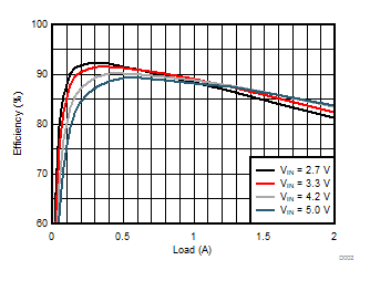
GUID-F6B73629-1CB8-4AA8-83CB-6BAEAEA75070-low.gif
VOUT = 1.2 V
Figure 9-3 Efficiency, Forced PWM Mode (2.0 MHz)
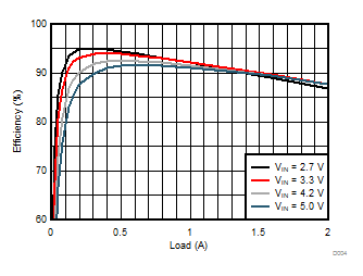
GUID-A59CDCE5-5C98-45DF-BC6A-3EBB95282580-low.gif
VOUT = 1.8 V
Figure 9-5 Efficiency, Forced PWM Mode (2.0 MHz)
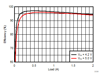
GUID-1CDE45F0-D7A9-4EC6-A4E2-2F4DC00E641E-low.gif
VOUT = 3.3 V
Figure 9-7 Efficiency, Forced PWM Mode (2.0 MHz)
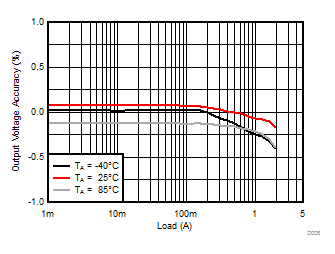
GUID-B5CF0C35-5973-4087-A1B7-D16D724064EC-low.gif
VOUT = 1.2 V
Figure 9-9 Load Regulation, Forced PWM Mode (2.0 MHz)
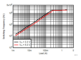
GUID-91D1B88D-B8C6-4DDD-9D6C-221C72AA092F-low.gif
VOUT = 1.2 V MODE = AGND
Figure 9-11 Switching Frequency, PWM/PSM Mode (2.0 MHz)
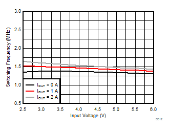
GUID-56E50529-B61E-4447-B065-901F7080030D-low.gif
VOUT = 1.2 V RMode = 8.2 kΩ
Figure 9-13 Switching Frequency, Forced PWM Mode (1.5 MHz)
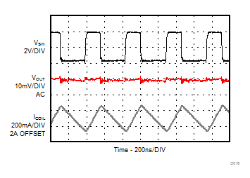
GUID-42645CFE-BCC0-4915-B6DE-11552D846D4B-low.gif
VOUT = 1.2 V IOUT = 2 A
Figure 9-15 Output Ripple, PWM Operation (2.0 MHz)
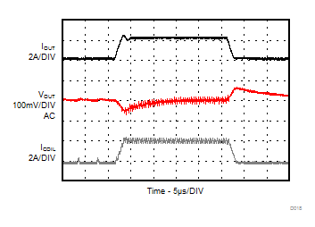
GUID-B3429BEF-6CE3-4461-9E1B-785C6CAD9B02-low.gif
VOUT = 1.2 V IOUT = 0 A to 2 A, 1 A / µs
Figure 9-17 Load Transient, PWM/PSM Mode (2.0 MHz)
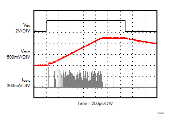
GUID-1704BC3F-5820-4A8F-9860-C5CCCB7FC161-low.gif
VOUT = 1.2 V ROUT = No Load
Figure 9-19 Startup and Shutdown without Load
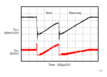
GUID-655B5955-25EE-4251-BE3A-F1557325AE4D-low.gif
VOUT = 1.2 V ROUT = 0.8 Ω (1.5 A) with 1-ms short
Figure 9-21 Short Circuit Protection, HICCUP