SLVSCD6A December 2015 – January 2021 TPS62097
PRODUCTION DATA
- 1 Features
- 2 Applications
- 3 Description
- 4 Revision History
- 5 Device Options
- 6 Pin Configuration and Functions
- 7 Specifications
- 8 Detailed Description
- 9 Application and Implementation
- 10Power Supply Recommendations
- 11Layout
- 12Device and Documentation Support
- 13Mechanical, Packaging, and Orderable Information
Package Options
Mechanical Data (Package|Pins)
- RWK|11
Thermal pad, mechanical data (Package|Pins)
Orderable Information
3 Description
The TPS62097 device is a synchronous step-down converter optimized for high efficiency and noise critical applications. The devices focus on high efficiency conversion over a wide output current range. At medium to heavy loads, the converter operates in PWM mode and automatically enters Power Save Mode operation at light load. The switching frequency is selectable in the range of 1.5 MHz to 2.5 MHz by an external resistor. iDCS-Control is able to be operated in forced PWM mode for low noise operation with a fixed switching frequency.
To address the requirements of system power rails, the internal compensation circuit allows a large selection of external output capacitor values in excess of 150 µF. To control the inrush current during the start-up, the device provides a programmable soft start-up by an external capacitor connected to the SS/TR pin. The SS/TR pin is also used in voltage tracking configurations. The device integrates short circuit protection, power good and thermal shutdown features. The device is available in a 2-mm x 2-mm VQFN package.
The new product, TPS62851x, offers reduced BOM cost, smaller total solution size and other features.
| PART NUMBER | PACKAGE(1) | BODY SIZE (NOM) |
|---|---|---|
| TPS62097 | VQFN (11) | 2.0 mm x 2.0 mm |
| TPS6209718 | ||
| TPS6209733 |
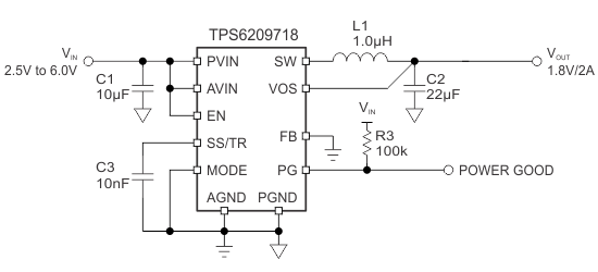
 1.8-V Output, PWM/PSM Mode
Application
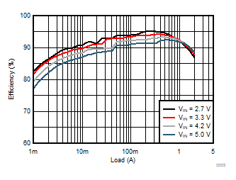
 1.8-V Output, PWM/PSM Mode
Efficiency