SLVSCD6A December 2015 – January 2021 TPS62097
PRODUCTION DATA
- 1 Features
- 2 Applications
- 3 Description
- 4 Revision History
- 5 Device Options
- 6 Pin Configuration and Functions
- 7 Specifications
- 8 Detailed Description
- 9 Application and Implementation
- 10Power Supply Recommendations
- 11Layout
- 12Device and Documentation Support
- 13Mechanical, Packaging, and Orderable Information
Package Options
Mechanical Data (Package|Pins)
- RWK|11
Thermal pad, mechanical data (Package|Pins)
Orderable Information
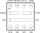
6 Pin Configuration and Functions
 Figure 6-1 11-Pin
VQFNRWK Package(Top View)
Figure 6-1 11-Pin
VQFNRWK Package(Top View)Table 6-1 Pin Functions
| PIN | I/O | DESCRIPTION | |
|---|---|---|---|
| NAME | NO. | ||
| PGND | 1 | Power ground pin | |
| SW | 2 | PWR | Switch pin. It is connected to the internal MOSFET switches. Connect the external inductor between this terminal and the output capacitor. |
| VOS | 3 | I | Output voltage sense pin. This pin must be directly connected to the output capacitor. |
| FB | 4 | I | Feedback pin. For the fixed output voltage versions, this pin is recommended to be connected to AGND for improved thermal performance. The pin also can be left floating as an internal 400-kΩ resistor is connected between this pin and AGND for fixed output voltage versions. For the adjustable output voltage version, a resistor divider sets the output voltage. |
| PG | 5 | O | Power-good open-drain output pin. The pullup resistor should not be connected to any voltage higher than 6 V. If it is not used, leave the pin floating. |
| EN | 6 | I | Enable pin. To enable the device, this pin needs to be pulled high. Pulling this pin low disables the device. This pin has an internal pulldown resistor of typically 375 kΩ when the device is disabled. |
| PVIN | 7 | PWR | Power input supply pin |
| AVIN | 8 | I | Analog input supply pin. Connect it to the PVIN pin together. |
| SS/TR | 9 | I | Soft start-up and voltage tracking pin. A capacitor is connected to this pin to set the soft start-up time. Leaving this pin floating sets the minimum start-up time. |
| MODE | 10 | I | Mode selection pin. Connect this pin to AGND to enable Power Save Mode with automatic transition between PWM and Power Save Mode. Connect this pin to an external resistor or leave floating to enable forced PWM mode only. See Table 8-1. |
| AGND | 11 | Analog ground pin | |