SLVSD86B december 2015 – may 2023 TPS65265
PRODUCTION DATA
- 1
- 1 Features
- 2 Applications
- 3 Description
- 4 Revision History
- 5 Device Comparison Table
- 6 Pin Configuration and Functions
- 7 Specifications
-
8 Detailed Description
- 8.1 Overview
- 8.2 Functional Block Diagram
- 8.3
Feature Description
- 8.3.1 Adjusting the Output Voltage
- 8.3.2 Mix PGOOD, PG_DLY Functions
- 8.3.3 Enable and Adjusting UVLO
- 8.3.4 Soft-Start Time
- 8.3.5 Power-Up Sequencing
- 8.3.6 V7V Low Dropout Regulator and Bootstrap
- 8.3.7 Out of Phase Operation
- 8.3.8 Output Overvoltage Protection (OVP)
- 8.3.9 PSM
- 8.3.10 Slope Compensation
- 8.3.11 Overcurrent Protection
- 8.3.12 Adjustable Switching Frequency
- 8.3.13 Thermal Shutdown
- 8.4 Device Functional Modes
- 9 Application and Implementation
- 10Device and Documentation Support
- 11Mechanical, Packaging, and Orderable Information
Package Options
Mechanical Data (Package|Pins)
- RHB|32
Thermal pad, mechanical data (Package|Pins)
- RHB|32
Orderable Information
8.3.5.2 Automatic Power Sequencing
The TPS65265 starts with a predefined power-up and power-down sequence when MODE pin ties HIGH or ties to GND. As shown in Table 8-2, the sequence is determined by the different combinations of EN1 and EN2 status. EN3 is used to start and stop the converters. Figure 8-6 shows the power sequencing when MODE ties to GND, EN1, and EN2 are tied to HIGH.
An internal 3-µA pullup current source is connected to SEQ_DLY pin. The interval time between bucks can be programmed by connecting a capacitor between SEQ_DLY pin and ground. The interval time can be calculated with Equation 5.
Equation 5. 
Equation 6. 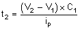
where
- V1 = 0.75 V
- V2 = 1.5 V
- Ip = 3 µA
Table 8-2 Power Sequencing
| MODE | EN1 | EN2 | EN3 | START SEQUENCING | SHUTDOWN SEQUENCING | |
|---|---|---|---|---|---|---|
| Automatic Power Sequencing | Connect to GND | High | High | Used to start and stop bucks in sequence | buck1 → buck2 → buck3 | buck3 → buck2 → buck1 |
| Connect to GND | Low | High | buck2 → buck1 → buck3 | buck3 → buck1 → buck2 | ||
| Connect to GND | High | Low | buck2 → buck3 → buck1 | buck1 → buck3 → buck2 | ||
| Connect to high or float | High | High | buck1 → buck3 → buck2 | buck2 → buck3 → buck1 | ||
| Connect to high or float | Low | High | buck3 → buck1 → buck2 | buck2 → buck1 → buck3 | ||
| Connect to high or float | High | Low | buck3 → buck2 → buck1 | buck1 → buck2 → buck3 | ||
| Connect to GND | Low | Low | Reserved | Reserved | Reserved | |
| Connect to high or float | Low | Low | Reserved | Reserved | Reserved | |
| Externally Controlled Sequencing | Floating | Used to start and stop buck1 | Used to start and stop buck2 | Used to start and stop buck3 | x | x |
 Figure 8-6 Automatic Power Sequencing