SLVSD86B december 2015 – may 2023 TPS65265
PRODUCTION DATA
- 1
- 1 Features
- 2 Applications
- 3 Description
- 4 Revision History
- 5 Device Comparison Table
- 6 Pin Configuration and Functions
- 7 Specifications
-
8 Detailed Description
- 8.1 Overview
- 8.2 Functional Block Diagram
- 8.3
Feature Description
- 8.3.1 Adjusting the Output Voltage
- 8.3.2 Mix PGOOD, PG_DLY Functions
- 8.3.3 Enable and Adjusting UVLO
- 8.3.4 Soft-Start Time
- 8.3.5 Power-Up Sequencing
- 8.3.6 V7V Low Dropout Regulator and Bootstrap
- 8.3.7 Out of Phase Operation
- 8.3.8 Output Overvoltage Protection (OVP)
- 8.3.9 PSM
- 8.3.10 Slope Compensation
- 8.3.11 Overcurrent Protection
- 8.3.12 Adjustable Switching Frequency
- 8.3.13 Thermal Shutdown
- 8.4 Device Functional Modes
- 9 Application and Implementation
- 10Device and Documentation Support
- 11Mechanical, Packaging, and Orderable Information
Package Options
Mechanical Data (Package|Pins)
- RHB|32
Thermal pad, mechanical data (Package|Pins)
- RHB|32
Orderable Information
3 Description
The TPS65265 incorporates triple synchronous buck converters with 4.5-V to 17-V wide input voltage range that encompassed most intermediate bus voltage operating off 5-, 9-, 12- or 15-V power bus or battery. The converter with constant frequency peak current mode is designed to simplify its application while giving designers options to optimize the system according to targeted applications. The switching frequency of the converters can be adjustable from 250 kHz to 2.3 MHz with an external resistor or external clock. 120° out-of-phase operation between Buck1, Buck2, and Buck3 minimizes the input filter requirements.
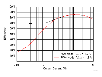
The TPS65265 operates in pulse skipping mode (PSM) with driving MODE pin to high or leaving float and operates in force continuous current mode (FCC) with connecting MODE pin to GND. PSM mode provides high efficiency by reducing switching losses at light load and FCC mode reduces noise susceptibility and RF interference.
The TPS65265 is available in a 32-pin thermal enhanced QFN (RHB) 5-mm × 5-mm thin package.
| PART NUMBER | PACKAGE | BODY SIZE (NOM) |
|---|---|---|
| TPS65265 | RHB (VQFN, 32) | 5.00 mm × 5.00 mm |
 Simplified Application Circuit
 Efficiency vs Output Load