SLVSD86B december   2015  – may 2023 TPS65265

PRODUCTION DATA  

  1.   1
  2. Features
  3. Applications
  4. Description
  5. Revision History
  6. Device Comparison Table
  7. Pin Configuration and Functions
  8. Specifications
    1. 7.1 Absolute Maximum Ratings
    2. 7.2 ESD Ratings
    3. 7.3 Recommended Operating Conditions
    4. 7.4 Thermal Information
    5. 7.5 Electrical Characteristics
    6. 7.6 Typical Characteristics
  9. Detailed Description
    1. 8.1 Overview
    2. 8.2 Functional Block Diagram
    3. 8.3 Feature Description
      1. 8.3.1  Adjusting the Output Voltage
      2. 8.3.2  Mix PGOOD, PG_DLY Functions
        1. 8.3.2.1 Programmable PGOOD DELAY
        2. 8.3.2.2 Relay Control
      3. 8.3.3  Enable and Adjusting UVLO
      4. 8.3.4  Soft-Start Time
      5. 8.3.5  Power-Up Sequencing
        1. 8.3.5.1 External Power Sequencing
        2. 8.3.5.2 Automatic Power Sequencing
      6. 8.3.6  V7V Low Dropout Regulator and Bootstrap
      7. 8.3.7  Out of Phase Operation
      8. 8.3.8  Output Overvoltage Protection (OVP)
      9. 8.3.9  PSM
      10. 8.3.10 Slope Compensation
      11. 8.3.11 Overcurrent Protection
        1. 8.3.11.1 High-Side MOSFET Overcurrent Protection
        2. 8.3.11.2 Low-Side MOSFET Overcurrent Protection
      12. 8.3.12 Adjustable Switching Frequency
      13. 8.3.13 Thermal Shutdown
    4. 8.4 Device Functional Modes
      1. 8.4.1 Operation With VIN < 4 V (Minimum VIN)
      2. 8.4.2 Operation With EN Control
  10. Application and Implementation
    1. 9.1 Application Information
    2. 9.2 Typical Application
      1. 9.2.1 Design Requirements
      2. 9.2.2 Detailed Design Procedure
        1. 9.2.2.1 Output Inductor Selection
        2. 9.2.2.2 Output Capacitor Selection
        3. 9.2.2.3 Input Capacitor Selection
        4. 9.2.2.4 Loop Compensation
      3. 9.2.3 Application Curves
    3. 9.3 Power Supply Recommendations
    4. 9.4 Layout
      1. 9.4.1 Layout Guidelines
      2. 9.4.2 Layout Example
  11. 10Device and Documentation Support
    1. 10.1 Receiving Notification of Documentation Updates
    2. 10.2 Support Resources
    3. 10.3 Trademarks
    4. 10.4 Electrostatic Discharge Caution
    5. 10.5 Glossary
  12. 11Mechanical, Packaging, and Orderable Information

Package Options

Mechanical Data (Package|Pins)
Thermal pad, mechanical data (Package|Pins)
Orderable Information

Typical Characteristics
GUID-1C11B1C9-F657-4253-9590-1C49BF45CBB2-low.gif
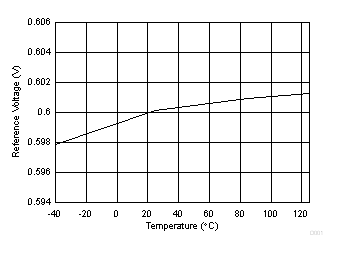
Figure 7-1 Voltage Reference vs Temperature
GUID-7DE1CDDE-542B-49A1-A5B0-AE158D2793A7-low.gif
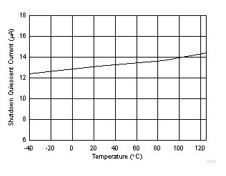
Figure 7-3 Shutdown Quiescent vs Temperature
GUID-5F43955A-F1E8-4029-95DB-5DCF53FAD5F6-low.gif
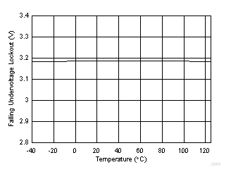
Figure 7-5 Vin UVLO Falling vs Temperature
GUID-570DEE2F-9CCD-4FF2-ADB9-A14D67B0CD59-low.gif
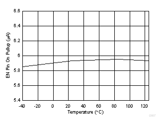
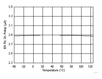
Figure 7-7 EN Pin Pullup Current vs Temperature, EN = 1.5 V
GUID-1B571505-94F4-4910-8079-5C3660D89019-low.gif
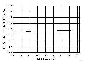
Figure 7-9 EN Pin Threshold Falling vs Temperature
GUID-25F4CDA2-6C55-4E09-9D33-F2B052FCA762-low.gif
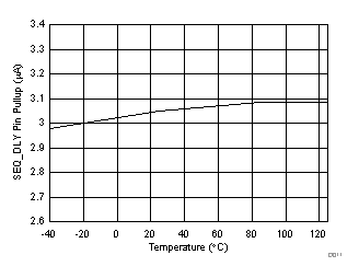
Figure 7-11 SEQ_DLY Pin Pullup Current vs Temperature, PG_DLY = 0.5 V
GUID-1E1E9AAC-4629-4869-A3BC-39B4E561F3B3-low.gif
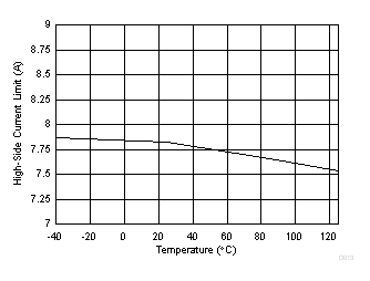
Figure 7-13 Buck1 High-Side Current Limit vs Temperature
GUID-92A281C3-DDAD-44D9-BFDA-4F0A718B21A8-low.gif
Figure 7-15 Buck3 High-Side Current Limit vs Temperature
GUID-6AFE85CA-E8CA-4ACF-A883-F326714392D3-low.gif
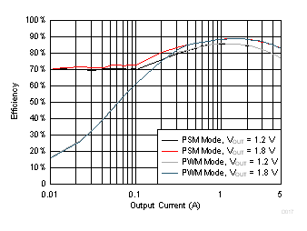
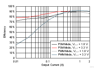
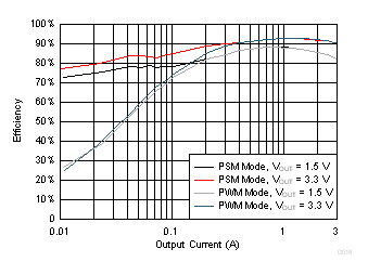
Figure 7-17 Buck1 Efficiency, VIN = 12 V, Fsw = 610 kHz
GUID-494205E0-49A0-4C94-A41C-EEAAA85DA085-low.gif
Figure 7-19 Buck3 Efficiency, VIN = 12 V, Fsw = 610 kHz
GUID-37D862C3-FD80-4D6D-B8A4-F6A9540253E1-low.gif
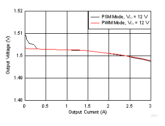
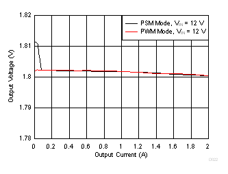
Figure 7-21 Buck2, Load Regulation
GUID-6DC63BDC-3113-4611-8035-4ED89828F052-low.gif
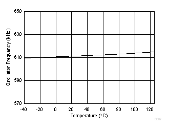
Figure 7-2 Oscillator Frequency vs Temperature
GUID-34AE22A6-79A6-4166-B886-67F3E08771C3-low.gif
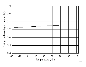
Figure 7-4 Vin UVLO Raising vs Temperature
GUID-87283D60-5FF0-494B-9868-FFB968AB2A5B-low.gif
Figure 7-6 EN Pin Pullup Current vs Temperature, EN = 1.0 V
GUID-B31CD2CD-FD93-465B-988A-4106B181102B-low.gif
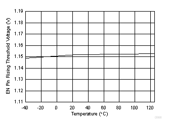
Figure 7-8 EN Pin Threshold Raising vs Temperature
GUID-E354CE42-9257-4E99-9997-A83402CB953A-low.gif
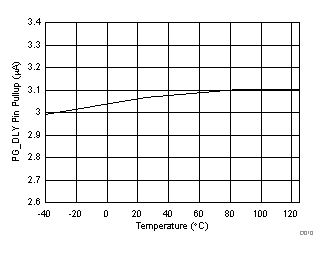
Figure 7-10 PG_DLY Pin Pullup Current vs Temperature, PG_DLY = 0.5 V
GUID-374581EF-F395-4DED-BBAA-074B7A31CB1C-low.gif
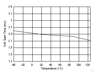
Figure 7-12 Soft-Start Time vs Temperature
GUID-3D8D287D-8F16-41C9-A032-5FCE182C8A8A-low.gif
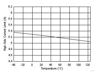
Figure 7-14 Buck2 High-Side Current Limit vs Temperature
GUID-3FFC6ADE-EF45-4585-AE6A-0EC941969398-low.gif
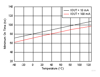
Figure 7-16 Minimum On Time vs Temperature
GUID-7F09D2FE-6F68-4A4D-BC61-750F5F1EA8A1-low.gif
Figure 7-18 Buck2 Efficiency, VIN = 12 V, Fsw = 610 kHz
GUID-9C284151-A7A0-494B-B181-2B2D26463B86-low.gif
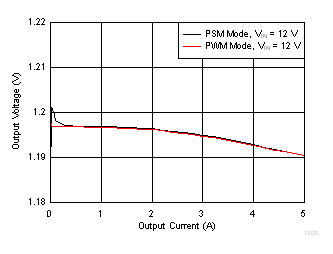
Figure 7-20 Buck1, Load Regulation
GUID-1944B26E-4E45-44C9-9C1D-E3F182D16ED5-low.gif
Figure 7-22 Buck3, Load Regulation