SBVS336C september 2021 – june 2023 TPS7A94
PRODUCTION DATA
- 1
- 1 Features
- 2 Applications
- 3 Description
- 4 Revision History
- 5 Pin Configuration and Functions
- 6 Specifications
-
7 Detailed Description
- 7.1 Overview
- 7.2 Functional Block Diagram
- 7.3
Feature Description
- 7.3.1 Output Voltage Setting and Regulation
- 7.3.2 Ultra-Low Noise and Ultra-High Power-Supply Rejection Ratio (PSRR)
- 7.3.3 Programmable Current Limit and Power-Good Threshold
- 7.3.4 Programmable Soft Start (NR/SS Pin)
- 7.3.5 Precision Enable and UVLO
- 7.3.6 Active Discharge
- 7.3.7 Thermal Shutdown Protection (TSD)
- 7.4 Device Functional Modes
-
8 Application and Implementation
- 8.1
Application Information
- 8.1.1 Output Voltage Restart (Overshoot Prevention Circuit)
- 8.1.2 Precision Enable (External UVLO)
- 8.1.3 Undervoltage Lockout (UVLO) Operation
- 8.1.4 Dropout Voltage (VDO)
- 8.1.5 Power-Good Feedback (FB_PG Pin) and Power-Good Threshold (PG Pin)
- 8.1.6 Adjusting the Factory-Programmed Current Limit
- 8.1.7 Programmable Soft-Start and Noise-Reduction (NR/SS Pin)
- 8.1.8 Inrush Current
- 8.1.9 Optimizing Noise and PSRR
- 8.1.10 Adjustable Operation
- 8.1.11 Paralleling for Higher Output Current and Lower Noise
- 8.1.12 Recommended Capacitor Types
- 8.1.13 Load Transient Response
- 8.1.14 Power Dissipation (PD)
- 8.1.15 Estimating Junction Temperature
- 8.1.16 TPS7A94EVM-046 Thermal Analysis
- 8.2 Typical Application
- 8.3 Power Supply Recommendations
- 8.4 Layout
- 8.1
Application Information
- 9 Device and Documentation Support
- 10Mechanical, Packaging, and Orderable Information
Package Options
Refer to the PDF data sheet for device specific package drawings
Mechanical Data (Package|Pins)
- DSC|10
Thermal pad, mechanical data (Package|Pins)
Orderable Information
8.1.6 Adjusting the Factory-Programmed Current Limit
Prior to start up, the input impedance of the FB_PG pin is sampled and the ICL value is adjusted based on the input impedance.
The current limit programmability is dependent on the output voltage. For voltages below 0.4 V, the current limit cannot be programmed. For voltages between 0.4 V and 1.2 V, the current limit cannot be adjusted and is always set to 100%. Table 8-1 describes this behavior.
| NOMINAL OUTPUT VOLTAGE (V) | RFB_PG(BOTTOM) (kΩ) | RFB_PG(TOP) (kΩ) | ICL SETTING (%) |
|---|---|---|---|
| VOUT(nom) ≥ 1.2 V |
RFB_PG(BOTTOM) = 0.2 V
/ 16 μA
|
RFB_PG(TOP) = RFB_PG(BOTTOM) × (
VOUT(nom) / 0.2 V × K – 1) with
K = PG threshold (%VOUT) |
100 |
|
RFB_PG(BOTTOM) = 0.2 V
/ 4 μA
|
80 | ||
|
RFB_PG(BOTTOM) = 0.2 V
/ 2 μA
|
60 | ||
| 0.4 V ≤ VOUT(nom) < 1.2 V |
RFB_PG(BOTTOM) = 0.2 V
/ 6 μA
|
100 | |
| VOUT(nom) < 0.4 V | N/A | N/A | N/A |
Table 8-2 provides values for various output voltages using 1% resistors.
| NOMINAL OUTPUT VOLTAGE (V) | RFB_PG(BOTTOM) (kΩ) | RFB_PG(TOP) (kΩ) | ICL SETTING (%) | PG THRESHOLD (%) |
|---|---|---|---|---|
| VOUT(nom) = 1.2 V | 12.4 | 51.1 | 100 | 85 |
| 49.9 | 205 | 80 | 85 | |
| 100 | 412 | 60 | 85 | |
| VOUT(nom) = 3.3 V | 12.4 | 187 | 100 | 95 |
| 49.9 | 732 | 80 | 95 | |
| 100 | 1470 | 60 | 95 | |
| VOUT(nom) = 5.1 V | 12.4 | 287 | 100 | 95 |
| 49.9 | 1150 | 80 | 95 | |
| 100 | 2320 | 60 | 95 |
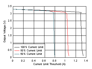
Figure 8-9 shows the different ICL settings for a nominal 3.3-V output voltage.
 Figure 8-9 Programmable Current Limit
Behavior (Typical) for a 3.3-VOUT(nom)