SLVSEW6F August 2021 – March 2024 TPS7H2211-SEP , TPS7H2211-SP
PRODUCTION DATA
- 1
- 1 Features
- 2 Applications
- 3 Description
- 4 Device Options
- 5 Related Products
- 6 Pin Configuration and Functions
-
7 Specifications
- 7.1 Absolute Maximum Ratings
- 7.2 ESD Ratings
- 7.3 Recommended Operating Conditions
- 7.4 Thermal Information
- 7.5 Electrical Characteristics: All Devices
- 7.6 Electrical Characteristics: CFP and KGD Options
- 7.7 Electrical Characteristics: HTSSOP Option
- 7.8 Switching Characteristics: All Devices
- 7.9 Quality Conformance Inspection
- 7.10 Typical Characteristics
- 8 Parameter Measurement Information
- 9 Detailed Description
- 10Application and Implementation
- 11Device and Documentation Support
- 12Revision History
- 13Mechanical, Packaging, and Orderable Information
Package Options
Refer to the PDF data sheet for device specific package drawings
Mechanical Data (Package|Pins)
- DAP|32
- KGD|0
- HKR|16
Thermal pad, mechanical data (Package|Pins)
- DAP|32
Orderable Information
10.2.2.2.2 Enable Control
The enable threshold is set by configuring the RBOT_EN and RTOP_EN resistors in order to turn on the switch at the desired input voltage as described in Section 9.3.1. For this design, the goal is to turn on the switch when VIN reaches 4.5 V. First we set RTOP_EN = 100 kΩ with a 0.1% tolerance resistor, and then use Equation 16 to calculate the nominal RBOT_EN. A 16.2-kΩ 0.1% tolerance resistor is found to best satisfy the equation.
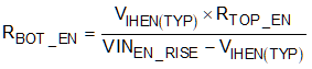
where
- VIHEN(TYP) = 0.63 V
- RTOP_EN = 100 kΩ
- VINEN_RISE = 4.5 V
Additionally, it should be ensured the worst case minimum and maximum turn-on voltages are acceptable. The minimum turn-on voltage would ideally be above 4.5 V (the minimum operating voltage). However, in this case that is not possible to achieve, and it is acceptable to allow the minimum turn-on voltage to be lower than 4.5 V (such as 4.2 V). Note however that the device will not be fully operational until at least 4.5 V is reached. This is okay in this case since the VIN voltage will quickly rise to above 4.5 V which puts the device in a fully operational state. The eFuse maximum turn-on voltage must be less than the minimum final VIN value (which is 4.9 V as determined by the 2% tolerance on the 5-V rail). The maximum turn-on voltage can be calculated using Equation 17. It is determined that VINEN_RISE(MAX) = 4.89 V which is under 4.9 V.

where
- VIHEN(MAX) = 0.68 V
- RTOP_EN = 100 kΩ
- RBOT_EN = 16.2 kΩ
- Rtolerance = 0.1% = 0.001
An alternative method to ensure the selected RBOT_EN value is acceptable for both the minimum and maximum enable thresholds is to select minimum and maximum values for VINEN_RISE and VINEN_FALL and ensure Equation 18 and Equation 19 are satisfied.


To summarize, using Equation 1 and Equation 2 with RTOP_EN = 100 kΩ and RBOT_EN = 16.2 kΩ, shows the eFuse will nominally turn on at 4.52 V and turn off at 3.73 V. The turn-off voltage is different due to the enable pin hysteresis. Taking into account the maximum and minimum EN pin thresholds and resistor tolerances the switch will turn on between 4.30 V and 4.89 V and turn off between 3.58 V and 4.10 V. To change the turn-off levels requires changing the turn-on levels. The turn-off level will act as an under voltage protection (UVP) feature to protect the downstream circuitry from receiving a sustained voltage under 3.58 V (which could potentially put the circuit in an undefined state).
Additionally, as the turn-on voltage minimum is 4.30 V, this is greater than 75% of the final VIN value (4.30 V > 4.9 V × 0.75 = 3.68 V). Therefore, there is no EN and slew rate related requirements as indicated in the electrical characteristics footnote (see Section 7.5). If the device was enabled under 3.68 V (not advised; this is less than the recommended operating VIN voltage of 4.5 V), the output voltage slew rate must be less than the input voltage slew rate or a false overcurrent trigger may occur.