SLVSEW6F August 2021 – March 2024 TPS7H2211-SEP , TPS7H2211-SP
PRODUCTION DATA
- 1
- 1 Features
- 2 Applications
- 3 Description
- 4 Device Options
- 5 Related Products
- 6 Pin Configuration and Functions
-
7 Specifications
- 7.1 Absolute Maximum Ratings
- 7.2 ESD Ratings
- 7.3 Recommended Operating Conditions
- 7.4 Thermal Information
- 7.5 Electrical Characteristics: All Devices
- 7.6 Electrical Characteristics: CFP and KGD Options
- 7.7 Electrical Characteristics: HTSSOP Option
- 7.8 Switching Characteristics: All Devices
- 7.9 Quality Conformance Inspection
- 7.10 Typical Characteristics
- 8 Parameter Measurement Information
- 9 Detailed Description
- 10Application and Implementation
- 11Device and Documentation Support
- 12Revision History
- 13Mechanical, Packaging, and Orderable Information
Package Options
Refer to the PDF data sheet for device specific package drawings
Mechanical Data (Package|Pins)
- DAP|32
- KGD|0
- HKR|16
Thermal pad, mechanical data (Package|Pins)
- DAP|32
Orderable Information
10.2.1.2.3 Overvoltage Protection
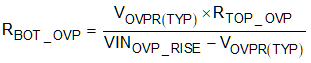
The overvoltage protection is set by configuring the RBOT_OVP and RTOP_OVP resistors. The overvoltage protection feature turns off the switch if the input voltage exceeds a predetermined value as described in Section 9.3.1. For this design, the goal is to have the overvoltage protection activate at a nominal voltage of 13.5 V. First set RTOP_OVP = 100 kΩ with a 0.1% tolerance resistor, then use Equation 10 to calculate the nominal value of RBOT_OVP. A nominal 9.31-kΩ 0.1% tolerance resistor best satisfies the equation.
where
- VOVPR(TYP) = 1.15 V
- RTOP_OVP = 100 kΩ
- VINOVP_RISE = 13.5 V
In order to ensure the selected RBOT_OVP value is acceptable for both the minimum and maximum OVP rising threshold, use Equation 11. VINOVP_RISE(MIN) is selected as the highest possible value that VIN will reach during nominal operation (to prevent false OVP trips). VINOVP_RISE(MAX) may be selected by the user as long as it is within the VIN of the Recommended Operating Conditions. These selections result in an allowable value of RBOT_OVP between 9.214 kΩ and 9.650 kΩ. The selected 9.31-kΩ 0.1% tolerance resistor satisfies these constraints, even when taking into account its tolerance.

where
- VOVPR(MAX) = 1.18 V
- RTOP_OVP = 100 kΩ
- Rtolerance = 0.01% = 0.001
- VINOVP_RISE(MAX) = 14 V
- VOVPR(MIN) = 1.11 V
- VINOVP_RISE(MIN) = VIN × (1 + tolerance) = 12.6 V
Since the OVP pin has hysteresis, the OVP falling threshold will be different than the rising threshold. Therefore, in order to ensure the selected RBOT_OVP value is acceptable for the OVP falling threshold, use Equation 12. VINOVP_FALL(MIN) and VINOVP_FALL(MAX) values may be selected using the same method as for VINOVP_RISE(MIN) and VINOVP_RISE(MAX). These selections results in an allowable RBOT_OVP value between of 9.129 kΩ and 9.460 kΩ. The selected 9.31-kΩ 0.1% tolerance resistor also satisfies these constraints, even when taking into account its tolerance.

where
- VOVPF(MAX) = 1.17 V
- RTOP_OVP = 100 kΩ
- Rtolerance = 0.001
- VINOVP_FALL(MAX) = 14 V
- VOVPF(MIN) = 1.09 V
- VINOVP_FALL(MIN) = VIN × (1 + tolerance) = 12.6 V
To summarize, using Equation 3 and Equation 4 with RTOP_OVP = 100 kΩ and RBOT_OVP = 9.31 kΩ, the eFuse will nominally go into overvoltage protection mode at 13.50 V and exit at 13.38 V. Taking into account the minimum and maximum OVP pin threshold and resistor tolerances, the switch will enter over voltage protection mode between 13.01 V and 13.88 V and exit between 12.77 V and 13.76 V.
The eFuse input voltage must remain within the recommended operating conditions (which contain a maximum VIN of 14 V). If OVP is configured above 14 V, then the OVP mode should only be used as a last resort feature. The eFuse is not intended to be above 14 V.