SLUSD49A September 2017 – January 2019 UCC256303
PRODUCTION DATA.
- 1 Features
- 2 Applications
- 3 Description
- 4 Revision History
- 5 Pin Configuration and Functions
- 6 Specifications
-
7 Detailed Description
- 7.1 Overview
- 7.2 Functional Block Diagram
- 7.3
Feature Description
- 7.3.1 Hybrid Hysteretic Control
- 7.3.2 Regulated 12-V Supply
- 7.3.3 Feedback Chain
- 7.3.4 Optocoupler Feedback Signal Input and Bias
- 7.3.5 System External Shut Down
- 7.3.6 Pick Lower Block and Soft Start Multiplexer
- 7.3.7 Pick Higher Block and Burst Mode Multiplexer
- 7.3.8 VCR Comparators
- 7.3.9 Resonant Capacitor Voltage Sensing
- 7.3.10 Resonant Current Sensing
- 7.3.11 Bulk Voltage Sensing
- 7.3.12 Output Voltage Sensing
- 7.3.13 High Voltage Gate Driver
- 7.3.14 Protections
- 7.4 Device Functional Modes
-
8 Application and Implementation
- 8.1 Application Information
- 8.2
Typical Application
- 8.2.1 Design Requirements
- 8.2.2
Detailed Design Procedure
- 8.2.2.1 LLC Power Stage Requirements
- 8.2.2.2 LLC Gain Range
- 8.2.2.3 Select Ln and Qe
- 8.2.2.4 Determine Equivalent Load Resistance
- 8.2.2.5 Determine Component Parameters for LLC Resonant Circuit
- 8.2.2.6 LLC Primary-Side Currents
- 8.2.2.7 LLC Secondary-Side Currents
- 8.2.2.8 LLC Transformer
- 8.2.2.9 LLC Resonant Inductor
- 8.2.2.10 LLC Resonant Capacitor
- 8.2.2.11 LLC Primary-Side MOSFETs
- 8.2.2.12 Design Considerations for Adaptive Dead-Time
- 8.2.2.13 LLC Rectifier Diodes
- 8.2.2.14 LLC Output Capacitors
- 8.2.2.15 BLK Pin Voltage Divider
- 8.2.2.16 BW Pin Voltage Divider
- 8.2.2.17 ISNS Pin Differentiator
- 8.2.2.18 VCR Pin Capacitor Divider
- 8.2.2.19 Burst Mode Programming
- 8.2.2.20 Soft-Start Capacitor
- 8.2.3 Application Curves
- 9 Power Supply Recommendations
- 10Layout
- 11Device and Documentation Support
- 12Mechanical, Packaging, and Orderable Information
Package Options
Refer to the PDF data sheet for device specific package drawings
Mechanical Data (Package|Pins)
- DDB|14
Thermal pad, mechanical data (Package|Pins)
Orderable Information
7.4.3 System States and Faults State Machine
Below is an overview of the system states sequence:
The state transition diagram starts from the un-powered condition of UCC256303. When PFC output voltage reaches a certain level, LLC is turned on. Before LLC starts running, the LO pin is kept high to pull the HS node of the LLC bridge low, thus allowing the capacitor between HB and HS pins to be charged from VCC via the bootstrap diode. UCC256303 will remain in the CHARGE_BOOT state for a certain time to ensure the boot capacitor is fully charged. When the load drops to below a certain level, LLC operates in burst mode
Fault conditions encountered by UCC256303 will cause operation to stop, or paused for a certain period of time followed by an automatic re-start. It is to ensure that while a persistent fault condition is present, it is not possible for UCC256303 or the power converter temperature to continue to rise as a result of the repeated re-start attempts.
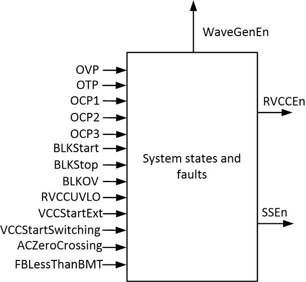
 Figure 38. Block Diagram of System States and Faults State Machine
 Table 1 summarizes the inputs and outputs of Figure 38
Table 1. System States and Faults State Machine Block Inputs and Outputs
| SIGNAL NAME | I/O | DESCRIPTION |
|---|---|---|
| OVP | I | Output over voltage fault |
| OTP | I | Over temperature fault |
| OCP1 | I | Peak current fault |
| OCP2 | I | Average current fault with 2ms timer |
| OCP3 | I | Average current fault with 50ms timer |
| BLKStart | I | Bulk voltage is above start threshold |
| BLKStop | I | Bulk voltage is below stop threshold |
| BLKOV | I | Bulk over voltage fault |
| RVCCUVLO | I | RVCC UVLO fault |
| VCCStartSwitching | I | VCC is above start switching threshold (the threshold is different in self bias mode and external bias mode) |
| ACZeroCrossing | I | AC zero crossing is detected |
| FBLessThanBMT | I | FBReplica voltage is less than burst mode threshold |
| WaveGenEn | O | Waveform generator enable |
| RVCCEn | O | RVCC enable |
| SSEn | O | Soft start enable |
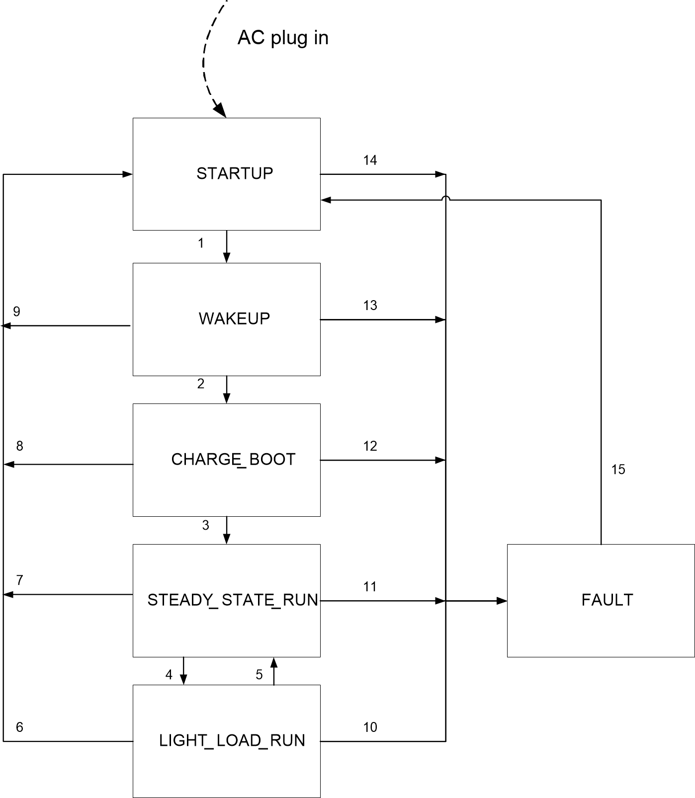
The state machine is shown in Figure 39 and the description of the states and state transition conditions are in the tables below.
 Figure 39. System States and Faults State Machine
 Table 2. States in System States and Faults State Machine
| STATE | OUTPUT STATUS | DESCRIPTION |
|---|---|---|
| STARTUP | WaveGenEn = 0
RVCCEn = 1 SSEn = 0 |
This is the first state after power on reset (POR).When VCC becomes higher than VCCstartswitching threshold, regulated RVCC is turned on to allow internal circuits to load trim settings and start up. |
| WAKEUP | WaveGenEn = 0
RVCCEn = 1 SSEn = 0 |
When BLK voltage reaches BLKStart level, the system enters WAKEUP state and stay in WAKEUP state for 150us for the analog circuits to wake up. |
| CHARGE_BOOT | WaveGenEn = 0
RVCCEn = 1 SSEn = 0 |
In this state, the BOOT capacitor is charged by turning on the low side switch for a certain period of time. |
| STEADY_STATE_RUN | WaveGenEn = 1
RVCCEn = 1 V SSEn = 1 |
In this state, the waveform generator is enabled. Soft start module is enabled. LLC starts to soft start. When soft start is done, the system enters normal operation. |
| LIGHT_LOAD_RUN | WaveGenEn = 1
RVCCEn = 1 SSEn = 1 |
If FBReplica is less than burst mode threshold during normal operation, the system enters LIGHT_LOAD_RUN mode. The FBLessThanBMT time is counted. If the time is longer than 200ms, it is treated as a fault, restart the system. |
| FAULT | WaveGenEn = 0
RVCCEn = 0 SSEn = 0 |
After any fault condition, the system enters FAULT state and waits for 1s before re-start. The 1s timer allows system to cool down and prevents frequent repetitive start up in case of a persistent fault. |
Table 3. System States and Faults State Machine State Transition Conditions
| STATE TRANSITION CONDITION | DESCRIPTION |
|---|---|
| 1 | System ready (trim load done)
VCCStartSwitching = 1 BLKStart = 1 BLKStop = 0 BLKOV = 0 RVCCUVLO = 0 |
| 2 | BLKStart = 1
BLKStop = 0 BLKOV = 0 RVCCUVLO = 0 FBLessThanBMT = 0 |
| 3 | Charge boot done |
| 4 | FBLessThanBMT = 1 |
| 5 | FBLessThanBMT = 0 |
| 6 | VCCStartSwitching = 0 or FBLessThanBMT time out |
| 7 | VCCStartSwitching = 0 |
| 8 | VCCStartSwitching = 0 or BLKOV = 1 |
| 9 | VCCStartSwitching = 0 or BLKOV = 1 |
| 10 | OTP = 1 or BLKOV = 1 or
BLKStop = 1 or OVP or OCP1 or OCP2 time out or OCP3 time out or RVCCUVLO = 1 |
| 11 | OTP = 1 or BLKOV = 1 or
BLKStop = 1 or OVP or OCP1 or OCP2 time out or OCP3 time out or RVCCUVLO = 1 |
| 12 | OTP = 1 |
| 13 | OTP = 1 |
| 14 | OTP = 1 |
| 15 | 1s pause time out |
Figure 40 only shows the most commonly used state transition (assuming no faults during start up states so all the states are captured in the timing diagram). Many different ways of state transitions may happen according to the state machine, but are not captured in this section.
In Figure 40, a normal start up procedure is shown. The system enters normal operation and then a fault (OCP, OVP, or OTP) happens.
NOTE
OCP1 and OVP are fast faults and are first processed in the waveform generator state machine.
The system is configured to be restart after 1s pause time.
 Figure 40. Timing Diagram of System States and Faults