SLUSDK4E may 2020 – july 2023 UCC28782
PRODUCTION DATA
- 1
- 1 Features
- 2 Applications
- 3 Description
- 4 Revision History
- 5 Device Comparison Table
- 6 Pin Configuration and Functions
- 7 Specifications
-
8 Detailed Description
- 8.1 Overview
- 8.2 Functional Block Diagram
- 8.3
Detailed Pin Description
- 8.3.1 BUR Pin (Programmable Burst Mode)
- 8.3.2 FB Pin (Feedback Pin)
- 8.3.3 REF Pin (Internal 5-V Bias)
- 8.3.4 VDD Pin (Device Bias Supply)
- 8.3.5 P13 and SWS Pins
- 8.3.6 S13 Pin
- 8.3.7 IPC Pin (Intelligent Power Control Pin)
- 8.3.8 RUN Pin (Driver and Bias Source for Isolator)
- 8.3.9 PWMH and AGND Pins
- 8.3.10 PWML and PGND Pins
- 8.3.11 SET Pin
- 8.3.12 RTZ Pin (Sets Delay for Transition Time to Zero)
- 8.3.13 RDM Pin (Sets Synthesized Demagnetization Time for ZVS Tuning)
- 8.3.14 BIN, BSW, and BGND Pins
- 8.3.15 XCD Pin
- 8.3.16 CS, VS, and FLT Pins
- 8.4
Device Functional Modes
- 8.4.1 Adaptive ZVS Control with Auto-Tuning
- 8.4.2 Dead-Time Optimization
- 8.4.3 EMI Dither and Dither Fading Function
- 8.4.4 Control Law across Entire Load Range
- 8.4.5 Adaptive Amplitude Modulation (AAM)
- 8.4.6 Adaptive Burst Mode (ABM)
- 8.4.7 Low Power Mode (LPM)
- 8.4.8 First Standby Power Mode (SBP1)
- 8.4.9 Second Standby Power Mode (SBP2)
- 8.4.10 Startup Sequence
- 8.4.11 Survival Mode of VDD (INT_STOP)
- 8.4.12 Capacitor Voltage Balancing Function
- 8.4.13 Device Functional Modes for Bias Regulator Control
- 8.4.14
System Fault Protections
- 8.4.14.1 Brown-In and Brown-Out
- 8.4.14.2 Output Over-Voltage Protection (OVP)
- 8.4.14.3 Input Over Voltage Protection (IOVP)
- 8.4.14.4 Over-Temperature Protection (OTP) on FLT Pin
- 8.4.14.5 Over-Temperature Protection (OTP) on CS Pin
- 8.4.14.6 Programmable Over-Power Protection (OPP)
- 8.4.14.7 Peak Power Limit (PPL)
- 8.4.14.8 Output Short-Circuit Protection (SCP)
- 8.4.14.9 Over-Current Protection (OCP)
- 8.4.14.10 External Shutdown
- 8.4.14.11 Internal Thermal Shutdown
- 8.4.15 Pin Open/Short Protections
-
9 Application and Implementation
- 9.1 Application Information
- 9.2
Typical Application Circuit
- 9.2.1 Design Requirements for a 65-W USB-PD Adapter Application
- 9.2.2
Detailed Design Procedure
- 9.2.2.1 Input Bulk Capacitance and Minimum Bulk Voltage
- 9.2.2.2 Transformer Calculations
- 9.2.2.3 Clamp Capacitor Calculation
- 9.2.2.4 Bleed-Resistor Calculation
- 9.2.2.5 Output Filter Calculation
- 9.2.2.6 Calculation of ZVS Sensing Network
- 9.2.2.7 Calculation of BUR Pin Resistances
- 9.2.2.8 Calculation of Compensation Network
- 9.2.3 Application Curves
- 10Power Supply Recommendations
- 11Layout
- 12Device and Documentation Support
- 13Mechanical, Packaging, and Orderable Information
Package Options
Mechanical Data (Package|Pins)
- RTW|24
Thermal pad, mechanical data (Package|Pins)
- RTW|24
Orderable Information
8.4.14.1 Brown-In and Brown-Out
The VS pin senses the negative voltage level of the auxiliary winding during the on-time of the primary-side switch (QL) to detect an under-voltage condition of the input DC or AC line. When the bulk voltage (VBULK) is too low, UCC28782 stops switching and no VO restart attempt is made until the input line voltage is back into normal range. As QL turns on with PWML, the negative voltage level of the auxiliary winding voltage (VAUX) is equal to VBULK divided by primary-to-auxiliary turns ratio (NPA) of the transformer, which is NP / NA. During this time, the voltage on VS pin is clamped to about 250 mV below AGND. As a result, VAUX can create a line-sensing current (IVSL) out of the VS pin flowing through the upper resistor of the voltage divider on VS pin (RVS1). With IVSL proportional to VBULK, it can be used to compare against two under-voltage thresholds, IVSL(RUN) and IVSL(STOP).
The following discussion, equations, and figures involving brown-in and brown-out thresholds are based on AC-line input conditions, but are generally applicable to DC input voltages as well. For an application using a DC input, substitute VDC(BI) for VAC(BI), VDC(BO) for VAC(BO) and remove the √2 factor from each equation and figure in this section.
The target brown-in AC voltage (VAC(BI)) can be programmed by the proper selection of RVS1. For every UVLO cycle of VDD, there are at least four initial test pulses from PWML to check IVSLcondition. IVSL of the first test pulse is ignored. If IVSL ≤ IVSL(RUN) is valid for the next three consecutive test pulses, the controller stops switching, the RUN pin goes low, and a new UVLO start cycle is initiated after VVDD reaches VVDD(OFF). On the other hand, if IVSL > IVSL(RUN) occurs, VO soft start sequence is initiated.
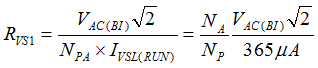
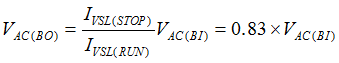
The brown-out AC voltage (VAC(BO)) is set internally by approximately 83% of VAC(BI), which provides enough hysteresis to compensate for possible sensing errors through the auxiliary winding.
A 60-ms timer (tBO) is used to bypass the effect of line ripple content on the IVSL sensing. Only when the IVSL ≤ IVSL(STOP) condition lasts longer than 60 ms (i.e. typically three line cycles of 50 Hz) and 3 additional switching cycles verify the condition, the brown-out fault is triggered. If switching is interrupted, the brown-out fault will remain pending without shut-down until the 3 verification cycles complete. The fault is reset after VVDD reaches VVDD(OFF). Figure 8-37 shows an example of the timing sequence of brown-out and brown-in protections for the case of an actual input brown-out condition. An application with DC input that has considerable ripple on the bulk voltage will behave similar to the AC-line bulk-ripple case.
 Figure 8-37 Timing Diagram of Brown-Out/Brown-In Response on AC Line Events
The tBO timer is started at the moment IVSL ≤ IVSL(STOP) is detected during the PWML on-time. The timer is cleared when IVSL > IVSL(STOP) is detected. In the case of an overshoot voltage on the output, switching will stop until the output voltage recovers to the regulation level. If the tBO timer is triggered by IVSL ≤ IVSL(STOP) while in the valley of the bulk ripple voltage, and then switching is stopped the status of IVSL cannot be detected and updated. The timer cannot be cleared without switching to sample IVSL, and the 60-ms timer may elapse even though no brown-out condition exists. To prevent an unwarranted shut-down, the 3 additional switching cycles sample the condition once switching does resume, to verify or dismiss the pending apparent brown-out fault. An extended output overshoot condition longer than tBO can result from a sudden load drop combined with a drop in the regulation reference due to reduction of cable compensation. Figure 8-38 shows an example of the timing sequence for the case of an apparent brown-out cancelled by 3 verifying pulses.
 Figure 8-38 Timing Diagram of Brown-Out Response on Extended Output Overshoot.