SLUS157Q December 1999 – October 2019 UCC1895 , UCC2895 , UCC3895
PRODUCTION DATA.
- 1 Features
- 2 Applications
- 3 Description
- 4 Revision History
- 5 Pin Configuration and Functions
- 6 Specifications
-
7 Detailed Description
- 7.1 Overview
- 7.2 Functional Block Diagrams
- 7.3
Feature Description
- 7.3.1 ADS (Adaptive Delay Set)
- 7.3.2 CS (Current Sense)
- 7.3.3 CT (Oscillator Timing Capacitor)
- 7.3.4 DELAB and DELCD (Delay Programming Between Complementary Outputs)
- 7.3.5 EAOUT, EAP, and EAN (Error Amplifier)
- 7.3.6 OUTA, OUTB, OUTC, and OUTD (Output MOSFET Drivers)
- 7.3.7 PGND (Power Ground)
- 7.3.8 RAMP (Inverting Input of the PWM Comparator)
- 7.3.9 REF (Voltage Reference)
- 7.3.10 RT (Oscillator Timing Resistor)
- 7.3.11 GND (Analog Ground)
- 7.3.12 SS/DISB (Soft Start/Disable)
- 7.3.13 SYNC (Oscillator Synchronization)
- 7.3.14 VDD (Chip Supply)
- 7.4 Device Functional Modes
- 7.5 Programming
-
8 Application and Implementation
- 8.1 Application Information
- 8.2
Typical Application
- 8.2.1 Design Requirements
- 8.2.2
Detailed Design Procedure
- 8.2.2.1 Power Loss Budget
- 8.2.2.2 Preliminary Transformer Calculations (T1)
- 8.2.2.3 QA, QB, QC, QD FET Selection
- 8.2.2.4 Selecting LS
- 8.2.2.5 Selecting Diodes DB and DC
- 8.2.2.6 Output Inductor Selection (LOUT)
- 8.2.2.7 Output Capacitance (COUT)
- 8.2.2.8 Select Rectifier Diodes
- 8.2.2.9 Input Capacitance (CIN)
- 8.2.2.10 Current Sense Network (CT, RCS, RR, DA)
- 8.2.3 Application Curves
- 9 Power Supply Recommendations
- 10Layout
- 11Device and Documentation Support
- 12Mechanical, Packaging, and Orderable Information
Package Options
Mechanical Data (Package|Pins)
Thermal pad, mechanical data (Package|Pins)
- PW|20
Orderable Information
6.5 Electrical Characteristics
VDD = 12 V, RT = 82 kΩ, CT = 220 pF, RDELAB = 10 kΩ, RDELCD = 10 kΩ, CREF = 0.1 μF, CVDD = 0.1 μF and no load on the outputs, TA = TJ. TA = 0°C to 70°C for UCC3895x, TA = –40°C to 85°C for UCC2895x and TA = –55°C to 125°C for the UCC1895x (unless otherwise noted)| PARAMETER | TEST CONDITIONS | MIN | TYP | MAX | UNIT | ||
|---|---|---|---|---|---|---|---|
| UVLO (UNDERVOLTAGE LOCKOUT) | |||||||
| UVLO(on) | Start-up voltage threshold | 10.2 | 11 | 11.8 | V | ||
| UVLO(off) | Minimum operating voltage after start-up | 8.2 | 9 | 9.8 | V | ||
| UVLO(hys) | Hysteresis | 1 | 2 | 3 | V | ||
| SUPPLY | |||||||
| ISTART | Start-up current | VDD = 8 V | 150 | 250 | µA | ||
| IDD | Operating current | 5 | 6 | mA | |||
| VDD_CLAMP | VDD clamp voltage | IDD = 10 mA | 16.5 | 17.5 | 18.5 | V | |
| VOLTAGE REFERENCE | |||||||
| VREF | Output voltage | TJ = 25°C | 4.94 | 5 | 5.06 | V | |
| 10 V < VDD < VDD_CLAMP,
0 mA < IREF < 5 mA, temperature |
4.85 | 5 | 5.15 | ||||
| ISC | Short circuit current | REF = 0 V, TJ = 25°C | 10 | 20 | mA | ||
| ERROR AMPLIFIER | |||||||
| Common-mode input voltage range | –0.1 | 3.6 | V | ||||
| VIO | Offset voltage | –7 | 7 | mV | |||
| IBIAS | Input bias current (EAP, EAN) | –1 | 1 | µA | |||
| EAOUT_VOH | High-level output voltage | EAP – EAN = 500 mV, IEAOUT = –0.5 mA | 4 | 4.5 | 5 | V | |
| EAOUT_VOL | Low-level output voltage | EAP – EAN = –500 mV, IEAOUT = 0.5 mA | 0 | 0.2 | 0.4 | V | |
| ISOURCE | Error amplifier output source current | EAP – EAN = 500 mV, EAOUT = 2.5 V | 1 | 1.5 | mA | ||
| ISINK | Error amplifier output sink current | EAP – EAN = –500 mV, EAOUT = 2.5 V | 2.5 | 4.5 | mA | ||
| AVOL | Open-loop dc gain | 75 | 85 | dB | |||
| GBW | Unity gain bandwidth(1) | 5 | 7 | mHz | |||
| Slew rate(1) | 1 V < EAN < 0 V, EAP = 500 mV,
0.5 V < EAOUT < 3 V |
1.5 | 2.2 | V/µs | |||
| No-load comparator turn-off threshold | 0.45 | 0.5 | 0.55 | V | |||
| No-load comparator turn-on threshold | 0.55 | 0.6 | 0.69 | V | |||
| No-load comparator hysteresis | 0.035 | 0.1 | 0.165 | V | |||
| OSCILLATOR | |||||||
| fOSC | Frequency | TJ = 25°C | 473 | 500 | 527 | kHz | |
| Frequency total variation | Over line, temperature | 2.5% | 5% | ||||
| VIH_SYNC | SYNC input threshold, SYNC | 2.05 | 2.1 | 2.4 | V | ||
| VOH_SYNC | High-level output voltage, SYNC | ISYNC = –400 μA, VCT = 2.6 V | 4.1 | 4.5 | 5 | V | |
| VOL_SYNC | Low-level output voltage, SYNC | ISYNC = 100 μA, VCT = 0 V | 0 | 0.5 | 1 | V | |
| Sync output pulse width | LOADSYNC = 3.9 kΩ and 30 pF in parallel | 85 | 135 | ns | |||
| VRT | Timing resistor voltage | 2.9 | 3 | 3.1 | V | ||
| VCT(peak) | Timing capacitor peak voltage | 2.25 | 2.35 | 2.55 | V | ||
| VCT(valley) | Timing capacitor valley voltage | 0 | 0.2 | 0.4 | V | ||
| CURRENT SENSE | |||||||
| ICS(bias) | Current sense bias current | 0 V < CS < 2.5 V,
0 V ADS < 2.5 V |
–4.5 | 20 | µA | ||
| Peak current threshold | 1.9 | 2 | 2.1 | V | |||
| Overcurrent threshold | 2.4 | 2.5 | 2.6 | V | |||
| Current sense to output delay | 0 V ≤ CS ≤ 2.3 V,
DELAB = DELCD = REF |
75 | 110 | ns | |||
| SOFT START/SHUTDOWN | |||||||
| ISOURCE | Soft-start source current | SS/DISB = 3.0 V,
CS = 1.9 V |
–40 | –35 | –30 | µA | |
| ISINK | Soft-start sink current | SS/DISB = 3.0 V,
CS = 2.6 V |
325 | 350 | 375 | µA | |
| Soft-start/disable comparator threshold | 0.44 | 0.5 | 0.56 | V | |||
| ADAPTIVE DELAY SET (ADS) | |||||||
| DELAB/DELCD output voltage | ADS = CS = 0 V | 0.45 | 0.5 | 0.55 | V | ||
| ADS = 0 V,
CS = 2 V |
1.9 | 2 | 2.1 | ||||
| tDELAY | Output delay(1)(3) | ADS = CS = 0 V | 450 | 560 | 620 | ns | |
| ADS bias current | 0 V < ADS < 2.5 V,
0 V < CS < 2.5 V |
–20 | 20 | µA | |||
| OUTPUT | |||||||
| VOH | High-level output voltage (all outputs) | IOUT = –10 mA, VDD to output | 250 | 400 | mV | ||
| VOL | Low-level output voltage (all outputs) | IOUT = 10 mA | UCC1895 | 150 | 300 | mV | |
| UCC2895, UCC3895 | 150 | 250 | |||||
| tR | Rise time(1) | CLOAD = 100 pF | 20 | 35 | ns | ||
| tF | Fall time(1) | CLOAD = 100 pF | 20 | 35 | ns | ||
| PWM COMPARATOR | |||||||
| EAOUT to RAMP input offset voltage | RAMP = 0 V,
DELAB = DELCD = REF |
0.72 | 0.85 | 1.05 | V | ||
| Minimum phase shift(2)
(OUTA to OUTC, OUTB to OUTD) |
RAMP = 0 V,
EAOUT = 650 mV |
0.0% | 0.85% | 1.4% | |||
| tDELAY | Delay(3)
(RAMP to OUTC, RAMP to OUTD) |
0 V < RAMP < 2.5 V, EAOUT = 1.2 V,
DELAB = DELCD = REF |
70 | 120 | ns | ||
| IR(bias) | RAMP bias current | RAMP < 5 V, CT = 2.2 V | –5 | 5 | µA | ||
| IR(sink) | RAMP sink current | RAMP = 5 V,
CT = 2.6 V |
UCC1895 | 10 | 19 | mA | |
| UCC2895, UCC3895 | 12 | 19 | |||||
(1) Ensured by design. Not production tested.
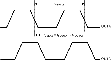
(2) Minimum phase shift is defined as:


- tf(OUTA) = falling edge of OUTA signal
- tf(OUTB) = falling edge of OUTB signal
- tf(OUTC) = falling edge of OUTC signal
- tf(OUTD) = falling edge of OUTD signal
- tPERIOD = period of OUTA or OUTB signal
where
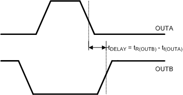
(3) Output delay is measured between OUTA and OUTB, or OUTC and OUTD. Output delay is defined as shown below where: tf(OUTA) = falling edge of OUTA signal, tr(OUTB) = rising edge of OUTB signal (see Figure 1 and Figure 2).
 Figure 1. Same Applies to OUTB and OUTD
  Figure 2. Same Applies to OUTC and OUTD