SLUSB72D March   2013  – April 2021 UCD3138064

PRODUCTION DATA  

  1. Features
  2. Applications
  3. Description
  4. Functional Block Diagram
  5. Revision History
  6. Device Options
    1. 6.1 Device Comparison Table
    2. 6.2 Product Selection Matrix
  7. Pin Configuration and Functions
    1. 7.1 Pin Diagrams
    2. 7.2 Pin Functions
  8. Specifications
    1. 8.1  Absolute Maximum Ratings (1)
    2. 8.2  Handling Ratings
    3. 8.3  Recommended Operating Conditions
    4. 8.4  Thermal Information
    5. 8.5  Electrical Characteristics
    6. 8.6  Timing Characteristics
    7. 8.7  PMBus/SMBus/I2C Timing
    8. 8.8  Power On Reset (POR) / Brown Out Reset (BOR)
    9. 8.9  Typical Clock Gating Power Savings
    10. 8.10 Typical Characteristics
  9. Detailed Description
    1. 9.1 Overview
      1. 9.1.1 ARM Processor
      2. 9.1.2 Memory
    2. 9.2 Functional Block Diagram
    3. 9.3 Feature Description
      1. 9.3.1  System Module
        1. 9.3.1.1 Address Decoder (DEC)
        2. 9.3.1.2 Memory Management Controller (MMC)
        3. 9.3.1.3 System Management (SYS)
        4. 9.3.1.4 Central Interrupt Module (CIM)
      2. 9.3.2  Peripherals
        1. 9.3.2.1 Digital Power Peripherals
          1. 9.3.2.1.1 Front End
          2. 9.3.2.1.2 DPWM Module
          3. 9.3.2.1.3 DPWM Events
          4. 9.3.2.1.4 High Resolution DPWM
          5. 9.3.2.1.5 Over Sampling
          6. 9.3.2.1.6 DPWM Interrupt Generation
          7. 9.3.2.1.7 DPWM Interrupt Scaling/Range
      3. 9.3.3  Automatic Mode Switching
        1. 9.3.3.1 Phase Shifted Full Bridge Example
        2. 9.3.3.2 LLC Example
        3. 9.3.3.3 Mechanism For Automatic Mode Switching
      4. 9.3.4  DPWMC, Edge Generation, Intramux
      5. 9.3.5  Filter
        1. 9.3.5.1 Loop Multiplexer
        2. 9.3.5.2 Fault Multiplexer
      6. 9.3.6  Communication Ports
        1. 9.3.6.1 SCI (UART) Serial Communication Interface
        2. 9.3.6.2 PMBUS/I2C
        3. 9.3.6.3 SPI
      7. 9.3.7  Real Time Clock
      8. 9.3.8  Timers
        1. 9.3.8.1 24-Bit Timer
        2. 9.3.8.2 16-Bit PWM Timers
        3. 9.3.8.3 Watchdog Timer
      9. 9.3.9  General Purpose ADC12
      10. 9.3.10 Miscellaneous Analog
      11. 9.3.11 Brownout
      12. 9.3.12 Global I/O
      13. 9.3.13 Temperature Sensor Control
      14. 9.3.14 I/O Mux Control
      15. 9.3.15 Current Sharing Control
      16. 9.3.16 Temperature Reference
    4. 9.4 Device Functional Modes
      1. 9.4.1 DPWM Modes Of Operation
        1. 9.4.1.1 Normal Mode
        2. 9.4.1.2 Phase Shifting
        3. 9.4.1.3 DPWM Multiple Output Mode
        4. 9.4.1.4 DPWM Resonant Mode
      2. 9.4.2 Triangular Mode
      3. 9.4.3 Leading Edge Mode
    5. 9.5 Memory
      1. 9.5.1 Register Maps
        1. 9.5.1.1 CPU Memory Map and Interrupts
          1. 9.5.1.1.1 Memory Map (After Reset Operation)
          2. 9.5.1.1.2 Memory Map (Normal Operation)
          3. 9.5.1.1.3 Memory Map (System and Peripherals Blocks)
        2. 9.5.1.2 Boot ROM
        3. 9.5.1.3 Customer Boot Program
        4. 9.5.1.4 Flash Management
        5. 9.5.1.5 Synchronous Rectifier MOSFET Ramp and IDE Calculation
  10. 10Applications and Implementation
    1. 10.1 Application Information
    2. 10.2 Typical Application
      1. 10.2.1 Design Requirements
      2. 10.2.2 Detailed Design Procedure
        1. 10.2.2.1 PCMC (Peak Current Mode Control) PSFB (Phase Shifted Full Bridge) Hardware Configuration Overview
        2. 10.2.2.2 DPWM Initialization for PSFB
          1. 10.2.2.2.1 DPWM Synchronization
        3. 10.2.2.3 Fixed Signals to Bridge
        4. 10.2.2.4 Dynamic Signals to Bridge
        5. 10.2.2.5 System Initialization for PCM
          1. 10.2.2.5.1 Use of Front Ends and Filters in PSFB
          2. 10.2.2.5.2 Peak Current Detection
          3. 10.2.2.5.3 Peak Current Mode (PCM)
      3. 10.2.3 Application Curves
  11. 11Power Supply Recommendations
    1. 11.1 Introduction To Power Supply and Layout Recommendations
    2. 11.2 3.3-V Supply Pins
    3. 11.3 Recommendation for V33 Ramp up Slew Rate for UCD3138 and UCD3138064
    4. 11.4 Recommendation for RC Time Constant of RESET Pin for UCD3138 and UCD3138064
  12. 12Layout
    1. 12.1 Layout Guidelines
      1. 12.1.1 EMI and EMC Mitigation Guidelines
      2. 12.1.2 BP18 Pin
      3. 12.1.3 Additional Bias Guidelines
      4. 12.1.4 UART Communication Port
    2. 12.2 Layout Example
      1. 12.2.1 UCD3138 and UCD3138064 40 Pin
      2. 12.2.2 UCD3138 and UCD3138064 64 Pin
  13. 13Device and Documentation Support
    1. 13.1 Device Support
    2. 13.2 Documentation Support
      1. 13.2.1 Related Documentation
    3. 13.3 Trademarks
    4. 13.4 Electrostatic Discharge Caution
    5. 13.5 Glossary
  14. 14Mechanical, Packaging, and Orderable Information

Package Options

Mechanical Data (Package|Pins)
Thermal pad, mechanical data (Package|Pins)
Orderable Information

Current Sharing Control

UCD3138x provides three separate modes of current sharing operation.

  • Analog bus current sharing
  • PWM bus current sharing
  • Master/Slave current sharing
  • AD02 has a special ESD protection mechanism that prevents the pin from pulling down the current-share bus if power is missing from the UCD3138x

The simplified current sharing circuitry is shown in the drawing below. The digital pulse connected to SW3 transforms SW3 into a pulse-width-modulated current source. Details on the frequency and resolution of this feature are in the digital power fusion peripherals manual.
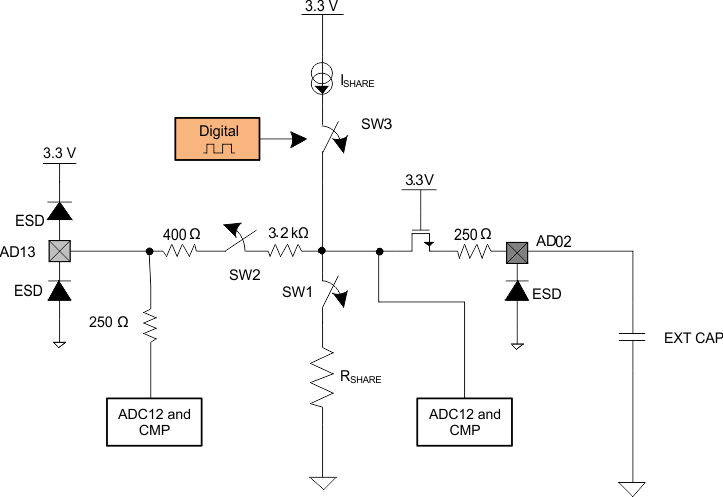
GUID-0086E1F7-6A68-43EB-AB10-1C35D46D0316-low.gifFigure 9-21 Simplified Current Sharing Circuitry
CURRENT SHARING MODEFOR TEST ONLY,
ALWAYS KEEP 00
CS_MODEEN_SW1EN_SW2DPWM
Off or Slave Mode (3-state)0000 (default)000
PWM Bus000110ACTIVE
Off or Slave Mode (3-state)0010000
Analog Bus or Master0011010

The period and the duty of 8-bit PWM current source and the state of the SW1 and SW2 switches can be controlled through the current sharing control register (CSCTRL).