SLUSB72D March 2013 – April 2021 UCD3138064
PRODUCTION DATA
- 1 Features
- 2 Applications
- 3 Description
- 4 Functional Block Diagram
- 5 Revision History
- 6 Device Options
- 7 Pin Configuration and Functions
-
8 Specifications
- 8.1 Absolute Maximum Ratings (1)
- 8.2 Handling Ratings
- 8.3 Recommended Operating Conditions
- 8.4 Thermal Information
- 8.5 Electrical Characteristics
- 8.6 Timing Characteristics
- 8.7 PMBus/SMBus/I2C Timing
- 8.8 Power On Reset (POR) / Brown Out Reset (BOR)
- 8.9 Typical Clock Gating Power Savings
- 8.10 Typical Characteristics
-
9 Detailed Description
- 9.1 Overview
- 9.2 Functional Block Diagram
- 9.3
Feature Description
- 9.3.1 System Module
- 9.3.2 Peripherals
- 9.3.3 Automatic Mode Switching
- 9.3.4 DPWMC, Edge Generation, Intramux
- 9.3.5 Filter
- 9.3.6 Communication Ports
- 9.3.7 Real Time Clock
- 9.3.8 Timers
- 9.3.9 General Purpose ADC12
- 9.3.10 Miscellaneous Analog
- 9.3.11 Brownout
- 9.3.12 Global I/O
- 9.3.13 Temperature Sensor Control
- 9.3.14 I/O Mux Control
- 9.3.15 Current Sharing Control
- 9.3.16 Temperature Reference
- 9.4 Device Functional Modes
- 9.5 Memory
-
10Applications and
Implementation
- 10.1 Application Information
- 10.2
Typical Application
- 10.2.1 Design Requirements
- 10.2.2 Detailed Design Procedure
- 10.2.3 Application Curves
- 11Power Supply Recommendations
- 12Layout
- 13Device and Documentation Support
- 14Mechanical, Packaging, and Orderable Information
Package Options
Mechanical Data (Package|Pins)
Thermal pad, mechanical data (Package|Pins)
Orderable Information
9.3.2.1.1 Front End
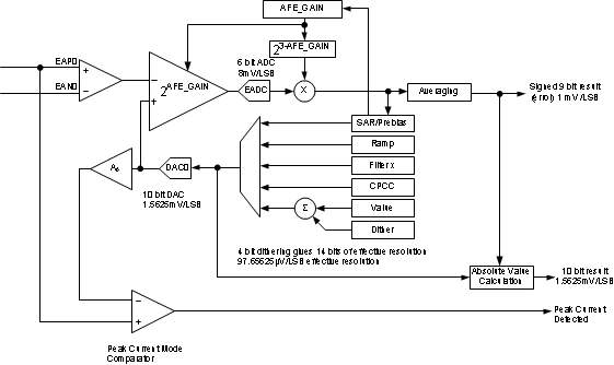
Figure 9-1 shows the block diagram of the front end module. It consists of a differential amplifier, an adjustable gain error amplifier, a high speed flash analog to digital converter (EADC), digital averaging filters and a precision high resolution set point DAC reference. The programmable gain amplifier in concert with the EADC and the adjustable digital gain on the EADC output work together to provide 9 bits of range with 6 bits of resolution on the EADC output. The output of the Front End module is a 9 bit sign extended result with a gain of 1 LSB / mV. Depending on the value of AFE selected, the resolution of this output could be either 1, 2, 4 or 8 LSBs. In addition Front End 0 has the ability to automatically select the AFE value such that the minimum resolution is maintained that still allows the voltage to fit within the range of the measurement. The EADC control logic receives the sample request from the DPWM module for initiating an EADC conversion. EADC control circuitry captures the EADC-9-bit-code and strobes the filter for processing of the representative error. The set point DAC has 10 bits with an additional 4 bits of dithering resulting in an effective resolution of 14 bits. This DAC can be driven from a variety of sources to facilitate things like soft start, nested loops, etc. Some additional features include the ability to change the polarity of the error measurement and an absolute value mode which automatically adds the DAC value to the error.
It is possible to operate the controller in a peak current mode control configuration. In this mode topologies like the phase shifted full bridge converter can be controlled to maintain transformer flux balance. The internal DAC can be ramped at a synchronously controlled slew rate to achieve a programmable slope compensation. This eliminates the sub-harmonic oscillation as well as improves input voltage feed-forward performance. A0 is a unity gain buffer used to isolate the peak current mode comparator. The offset of this buffer is specified in the Section 8.5 table.
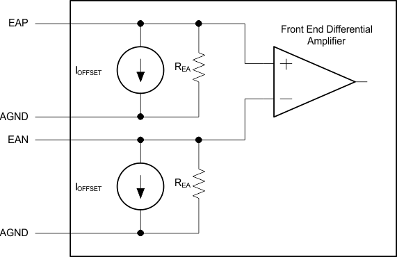
 Figure 9-1 Input Stage Of EADC Module
 Figure 9-2 Front End Module