SWRS170L March 2014 – May 2025 WL1807MOD , WL1837MOD
PRODUCTION DATA
- 1
- 1 Features
- 2 Applications
- 3 Description
- 4 Functional Block Diagram
- 5 Device Comparison
- 6 Pin Configuration and Functions
-
7 Specifications
- 7.1 Absolute Maximum Ratings
- 7.2 ESD Ratings
- 7.3 Recommended Operating Conditions
- 7.4 External Digital Slow Clock Requirements
- 7.5 Thermal Resistance Characteristics for MOC 100-Pin Package
- 7.6 WLAN Performance: 2.4GHz Receiver Characteristics
- 7.7 WLAN Performance: 2.4GHz Transmitter Power
- 7.8 WLAN Performance: 5GHz Receiver Characteristics
- 7.9 WLAN Performance: 5GHz Transmitter Power
- 7.10 WLAN Performance: Currents
- 7.11 Bluetooth Performance: BR, EDR Receiver Characteristics—In-Band Signals
- 7.12 Bluetooth Performance: Transmitter, BR
- 7.13 Bluetooth Performance: Transmitter, EDR
- 7.14 Bluetooth Performance: Modulation, BR
- 7.15 Bluetooth Performance: Modulation, EDR
- 7.16 Bluetooth Low Energy Performance: Receiver Characteristics – In-Band Signals
- 7.17 Bluetooth Low Energy Performance: Transmitter Characteristics
- 7.18 Bluetooth Low Energy Performance: Modulation Characteristics
- 7.19 Bluetooth BR and EDR Dynamic Currents
- 7.20 Bluetooth Low Energy Currents
- 7.21
Timing and Switching Characteristics
- 7.21.1 Power Management
- 7.21.2 Power-Up and SHUTDOWN States
- 7.21.3 Chip Top-level Power-Up Sequence
- 7.21.4 WLAN Power-Up Sequence
- 7.21.5 Bluetooth-Bluetooth Low Energy Power-Up Sequence
- 7.21.6 WLAN SDIO Transport Layer
- 7.21.7 HCI UART Shared-Transport Layers for All Functional Blocks (Except WLAN)
- 7.21.8 Bluetooth Codec-PCM (Audio) Timing Specifications
- 8 Detailed Description
- 9 Applications, Implementation, and Layout
- 10Device and Documentation Support
- 11Revision History
- 12Mechanical, Packaging, and Orderable Information
Package Options
Refer to the PDF data sheet for device specific package drawings
Mechanical Data (Package|Pins)
- MOC|100
Thermal pad, mechanical data (Package|Pins)
Orderable Information
7.21.6.1 SDIO Timing Specifications
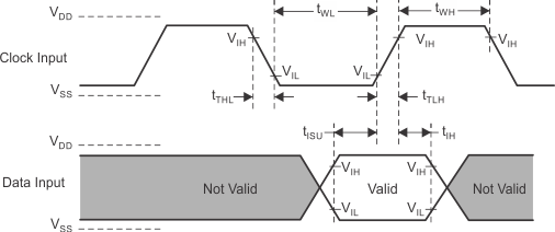
Figure 7-6 and Figure 7-7 show the SDIO switching characteristics over recommended operating conditions and with the default rate for input and output.
 Figure 7-6 SDIO Default Input Timing
 Figure 7-7 SDIO Default Output Timing
Table 7-1 lists the SDIO default timing characteristics.
Table 7-1 SDIO Default Timing Characteristics
| (1) | MIN | MAX | UNIT | |
|---|---|---|---|---|
| fclock | Clock frequency, CLK(2) | 0.0 | 26.0 | MHz |
| DC | Low, high duty cycle(2) | 40.0% | 60.0% | |
| tTLH | Rise time, CLK(2) | 10.0 | ns | |
| tTHL | Fall time, CLK(2) | 10.0 | ns | |
| tISU | Setup time, input valid before CLK ↑(2) | 3.0 | ns | |
| tIH | Hold time, input valid after CLK ↑(2) | 2.0 | ns | |
| tODLY | Delay time, CLK ↓ to output valid(2) | 7.0 | 10.0 | ns |
| Cl | Capacitive load on outputs(2) | 15.0 | pF | |
(1) To change the data out clock edge from the falling edge (default) to the rising edge, set the configuration bit.
(2) Parameter values reflect maximum clock frequency.