12ビット、RF サンプリング A/D コンバータ (ADC)" />

JAJSGI4B November   2018  – March 2021 ADC12DJ3200QML-SP

PRODUCTION DATA  

  1. 特長
  2. アプリケーション
  3. 概要
  4. Revision History
  5. Pin Configuration and Functions
  6. Specifications
    1. 6.1  Absolute Maximum Ratings
    2. 6.2  ESD Ratings
    3. 6.3  Recommended Operating Conditions
    4. 6.4  Thermal Information
    5. 6.5  Electrical Characteristics: DC Specifications
    6. 6.6  Electrical Characteristics: Power Consumption
    7. 6.7  Electrical Characteristics: AC Specifications (Dual-Channel Mode)
    8. 6.8  Electrical Characteristics: AC Specifications (Single-Channel Mode)
    9. 6.9  Timing Requirements
    10. 6.10 Switching Characteristics
    11. 6.11 Timing Diagrams
    12. 6.12 Typical Characteristics
  7. Detailed Description
    1. 7.1 Overview
    2. 7.2 Functional Block Diagram
    3. 7.3 Feature Description
      1. 7.3.1 Analog Inputs
        1. 7.3.1.1 Analog Input Protection
        2. 7.3.1.2 Full-Scale Voltage (VFS) Adjustment
        3. 7.3.1.3 Analog Input Offset Adjust
      2. 7.3.2 ADC Core
        1. 7.3.2.1 ADC Theory of Operation
        2. 7.3.2.2 ADC Core Calibration
        3. 7.3.2.3 ADC Overrange Detection
        4. 7.3.2.4 Code Error Rate (CER)
      3. 7.3.3 Timestamp
      4. 7.3.4 Clocking
        1. 7.3.4.1 Noiseless Aperture Delay Adjustment (tAD Adjust)
        2. 7.3.4.2 Aperture Delay Ramp Control (TAD_RAMP)
        3. 7.3.4.3 SYSREF Capture for Multi-Device Synchronization and Deterministic Latency
          1. 7.3.4.3.1 SYSREF Position Detector and Sampling Position Selection (SYSREF Windowing)
          2. 7.3.4.3.2 Automatic SYSREF Calibration
      5. 7.3.5 Digital Down Converters (Dual-Channel Mode Only)
        1. 7.3.5.1 Numerically-Controlled Oscillator and Complex Mixer
          1. 7.3.5.1.1 NCO Fast Frequency Hopping (FFH)
          2. 7.3.5.1.2 NCO Selection
          3. 7.3.5.1.3 Basic NCO Frequency Setting Mode
          4. 7.3.5.1.4 Rational NCO Frequency Setting Mode
          5. 7.3.5.1.5 NCO Phase Offset Setting
          6. 7.3.5.1.6 NCO Phase Synchronization
        2. 7.3.5.2 Decimation Filters
        3. 7.3.5.3 Output Data Format
        4. 7.3.5.4 Decimation Settings
          1. 7.3.5.4.1 Decimation Factor
          2. 7.3.5.4.2 DDC Gain Boost
      6. 7.3.6 JESD204B Interface
        1. 7.3.6.1 Transport Layer
        2. 7.3.6.2 Scrambler
        3. 7.3.6.3 Link Layer
          1. 7.3.6.3.1 Code Group Synchronization (CGS)
          2. 7.3.6.3.2 Initial Lane Alignment Sequence (ILAS)
          3. 7.3.6.3.3 8b, 10b Encoding
          4. 7.3.6.3.4 Frame and Multiframe Monitoring
        4. 7.3.6.4 Physical Layer
          1. 7.3.6.4.1 SerDes Pre-Emphasis
        5. 7.3.6.5 JESD204B Enable
        6. 7.3.6.6 Multi-Device Synchronization and Deterministic Latency
        7. 7.3.6.7 Operation in Subclass 0 Systems
      7. 7.3.7 Alarm Monitoring
        1. 7.3.7.1 NCO Upset Detection
        2. 7.3.7.2 Clock Upset Detection
      8. 7.3.8 Temperature Monitoring Diode
      9. 7.3.9 Analog Reference Voltage
    4. 7.4 Device Functional Modes
      1. 7.4.1 Dual-Channel Mode
      2. 7.4.2 Single-Channel Mode (DES Mode)
      3. 7.4.3 JESD204B Modes
        1. 7.4.3.1 JESD204B Output Data Formats
        2. 7.4.3.2 Dual DDC and Redundant Data Mode
      4. 7.4.4 Power-Down Modes
      5. 7.4.5 Test Modes
        1. 7.4.5.1 Serializer Test-Mode Details
        2. 7.4.5.2 PRBS Test Modes
        3. 7.4.5.3 Ramp Test Mode
        4. 7.4.5.4 Short and Long Transport Test Mode
          1. 7.4.5.4.1 Short Transport Test Pattern
          2. 7.4.5.4.2 Long Transport Test Pattern
        5. 7.4.5.5 D21.5 Test Mode
        6. 7.4.5.6 K28.5 Test Mode
        7. 7.4.5.7 Repeated ILA Test Mode
        8. 7.4.5.8 Modified RPAT Test Mode
      6. 7.4.6 Calibration Modes and Trimming
        1. 7.4.6.1 Foreground Calibration Mode
        2. 7.4.6.2 Background Calibration Mode
        3. 7.4.6.3 Low-Power Background Calibration (LPBG) Mode
      7. 7.4.7 Offset Calibration
      8. 7.4.8 Trimming
      9. 7.4.9 Offset Filtering
    5. 7.5 Programming
      1. 7.5.1 Using the Serial Interface
        1. 7.5.1.1 SCS
        2. 7.5.1.2 SCLK
        3. 7.5.1.3 SDI
        4. 7.5.1.4 SDO
        5. 7.5.1.5 Streaming Mode
    6. 7.6 Register Maps
      1. 7.6.1 Register Descriptions
      2. 7.6.2 SYSREF Calibration Registers (0x2B0 to 0x2BF)
      3. 7.6.3 Alarm Registers (0x2C0 to 0x2C2)
  8. Application Information Disclaimer
    1. 8.1 Application Information
      1. 8.1.1 Analog Inputs
      2. 8.1.2 Analog Input Bandwidth
      3. 8.1.3 Clocking
      4. 8.1.4 Radiation Environment Recommendations
        1. 8.1.4.1 Single Event Latch-Up (SEL)
        2. 8.1.4.2 Single Event Functional Interrupt (SEFI)
        3. 8.1.4.3 Single Event Upset (SEU)
    2. 8.2 Typical Application
      1. 8.2.1 Design Requirements
      2. 8.2.2 Detailed Design Procedure
        1. 8.2.2.1 RF Input Signal Path
        2. 8.2.2.2 Calculating Values of AC-Coupling Capacitors
      3. 8.2.3 Application Curves
    3. 8.3 Initialization Set Up
      1.      Power Supply Recommendations
        1. 9.1 Power Sequencing
  9. Layout
    1. 9.1 Layout Guidelines
    2. 9.2 Layout Example
  10. 10Device and Documentation Support
    1. 10.1 Device Support
      1. 10.1.1 Development Support
    2. 10.2 Documentation Support
      1. 10.2.1 Related Documentation
    3. 10.3 Receiving Notification of Documentation Updates
    4. 10.4 Community Resources
    5. 10.5 Trademarks
      1.      Mechanical, Packaging, and Orderable Information

パッケージ・オプション

デバイスごとのパッケージ図は、PDF版データシートをご参照ください。

メカニカル・データ(パッケージ|ピン)
  • ZMX|196
  • NWE|196
サーマルパッド・メカニカル・データ
発注情報

Calculating Values of AC-Coupling Capacitors

AC-coupling capacitors are used in the input CLK± and JESD204B output data pairs. The capacitor values must be large enough to address the lowest frequency signals of interest, but not so large as to cause excessively long startup biasing times, or unwanted parasitic inductance.

The minimum capacitor value can be calculated based on the lowest frequency signal that is transferred through the capacitor. Given a 50-Ω single-ended clock or data path impedance, good practice is to set the capacitor impedance to be <1 Ω at the lowest frequency of interest. This setting provides minimal impact on signal level at that frequency. For the CLK± path, the minimum-rated clock frequency is 800 MHz. Therefore, the minimum capacitor value can be calculated from:

Equation 12. GUID-C8525C6A-327B-4FBB-B072-61C55A50206C-low.gif

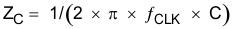
Setting Zc = 1 Ω and rearranging gives:

Equation 13. GUID-F48447AE-10D2-4359-87E9-81FDD56082A4-low.gif

Therefore, a capacitance value of at least 199 pF is needed to provide the low-frequency response for the CLK± path. If the minimum clock frequency is higher than 800 MHz, this calculation can be revisited for that frequency. Similar calculations can be done for the JESD204B output data capacitors based on the minimum frequency in that interface. Capacitors must also be selected for good response at high frequencies (low inductance) and with dimensions that match the high-frequency signal traces they are connected to. Capacitors of the 0201 size are frequently well suited to these applications.