JAJSSF8 December 2023 LDC5071-Q1
PRODUCTION DATA
- 1
- 1 特長
- 2 アプリケーション
- 3 概要
- 4 Pin Configuration and Functions
- 5 Specifications
- 6 Detailed Description
- 7 Application and Implementation
- 8 Device and Documentation Support
- 9 Revision History
- 10Mechanical, Packaging, and Orderable Information
6.3.3.3 Automatic Gain Control
When the voltage on the AGC_EN pin is below VAGC_EN_AUTO, the manual gain control function is disabled and the Automatic Gain Control (AGC) is enabled.
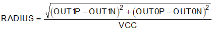
In AGC mode, the device will change the gain of the last stage of the signal processing block to keep the final output within an appropriate voltage range on VOUT. The AGC block uses the square root of the sum of the squared amplitudes of the two channels to sense amplitude of output signals and set gain selection. Both channels will have the same gain. This means that the AGC block will set the gain for sine and cosine channels such that the quantity AGC_TARGET as defined in Equation 8 is within the ranges listed in SpecificationsSpecificationsSpecifications.
where
- OUTxx: Voltage on the output pins
- VCC: Voltage on the VCC pin
- AGC_TARGET: Regulation target for the AGC block
The AGC sets the gain in the DIAGNOSTICS state and then dynamically regulates the gain in NORMAL state. There are two regions of regulation, the slow AGC regulation region and the fast AGC regulation region. See Figure 7-10. The blue curve shows the ratio defined by Equation 8 as percentage of VCC. If the ratio rises above AGC_FH or falls below AGC_FL, fast regulation becomes active, and the gain is changed by four gain codes every nominal value of 819.2 μs. If the ratio falls between AGC_SH and AGC_FH, or between AGC_FL and AGC_SL, slow regulation is active, and the gain is changed by one code approximately every 840 mS. To allow for faster settling of the output during power up in the diagnostic state, the device changes gain by one code every 3.2 μs in slow AGC region and eight codes every 3.2 μs in the fast AGC region. The thresholds are listed in SpecificationsSpecificationsSpecifications. The gain step size is constant in dB scale and is approximately equal to 0.15 dB. Figure 7-10 shows the two cases: a fast change (for example, due to a transient), and a slow change due to lifetime drift.
The AGC block thus will try to compensate for changes in amplitude of the input signal or changes in VCC. If the ratio, after reaching AGC_TARGET, stays between AGC_SH and AGC_SL, then AGC does not react and does not change the gain. The AGC block engages if one of the thresholds is crossed, and it will try to change the output amplitudes such that the ratio reaches AGC_TARGET again. Hence, the No Gain Control region in Figure 7-10 causes the AGC block to have some hysteresis.
 Figure 6-3 AGC Regulation Bands