JAJSRI9A October 2023 – March 2024 LM51772
ADVANCE INFORMATION
- 1
- 1 特長
- 2 アプリケーション
- 3 概要
- 4 概要 (続き)
- 5 Pin Configuration and Functions
- 6 Specifications
- 7 Parameter Measurement Information
-
8 Detailed Description
- 8.1 Overview
- 8.2 Functional Block Diagram
- 8.3
Feature Description
- 8.3.1 Buck-Boost Control Scheme
- 8.3.2 Power Save Mode
- 8.3.3 Programmable Conduction Mode PCM
- 8.3.4 Reference System
- 8.3.5 Supply Voltage Selection – VMAX Switch and Selection Logic
- 8.3.6 Enable and Undervoltage Lockout
- 8.3.7 Internal VCC Regulator
- 8.3.8 Error Amplifier and Control
- 8.3.9 Short Circuit - Hiccup Protection
- 8.3.10 Current Monitor/Limiter
- 8.3.11 Oscillator Frequency Selection
- 8.3.12 Frequency Synchronization
- 8.3.13 Output Voltage Tracking
- 8.3.14 Slope Compensation
- 8.3.15 Configurable Soft Start
- 8.3.16 Drive Pin
- 8.3.17 Dual Random Spread Spectrum – DRSS
- 8.3.18 Gate Driver
- 8.3.19 Cable Drop Compensation (CDC)
- 8.3.20 CFG-pin and R2D Interface
- 8.3.21 Advanced Monitoring Features
- 8.3.22
Protection Features
- 8.3.22.1 Thermal Shutdown (TSD)
- 8.3.22.2 Over Current Protection
- 8.3.22.3 Output Over Voltage Protection 1 (OVP1)
- 8.3.22.4 Output Over Voltage Protection 2 (OVP2)
- 8.3.22.5 Input Voltage Protection (IVP)
- 8.3.22.6 Input Voltage Regulation (IVR)
- 8.3.22.7 Power Good
- 8.3.22.8 Boot-Strap Under Voltage Protection
- 8.3.22.9 Boot-strap Over Voltage Clamp
- 8.3.22.10 CRC - CHECK
- 8.4 Device Functional Modes
- 8.5 Programming
- 9 LM51772 Registers
-
10Application and Implementation
- 10.1 Application Information
- 10.2
Typical Application
- 10.2.1 Design Requirements
- 10.2.2
Detailed Design Procedure
- 10.2.2.1 Custom Design with WEBENCH Tools
- 10.2.2.2 Frequency
- 10.2.2.3 Feedback Divider
- 10.2.2.4 Inductor and Current Sense Resistor Selection
- 10.2.2.5 Output Capacitor
- 10.2.2.6 Input Capacitor
- 10.2.2.7 Slope Compensation
- 10.2.2.8 UVLO Divider
- 10.2.2.9 Soft-Start Capacitor
- 10.2.2.10 MOSFETs QH1 and QL1
- 10.2.2.11 MOSFETs QH2 and QL2
- 10.2.2.12 Loop Compensation
- 10.2.2.13 External Component Selection
- 10.2.3 Application Curves
- 10.3 Power Supply Recommendations
- 10.4 Layout
- 11Device and Documentation Support
- 12Revision History
- 13Mechanical, Packaging, and Orderable Information
8.3.5 Supply Voltage Selection – VMAX Switch and Selection Logic
There are two pins to supply the LM51772 internal voltage regulators. Due to the internal supply voltage selection circuit, the device can reduce the power dissipation by ensuring a seamless operation at low input or output voltages as well as in transient operating conditions like an output short. The VMAX switch selects the pin with the lower voltage from the VIN or BIAS pin once the voltage on both is above the switch-over threshold (VT(VCC, SUP)). If one pin voltage is lower than the threshold, the other supply pin is selected. And if both pins are lower than the switch-over threshold, the higher voltage of VIN or BIAS is selected as supply. The following are common configurations for the supply pins:
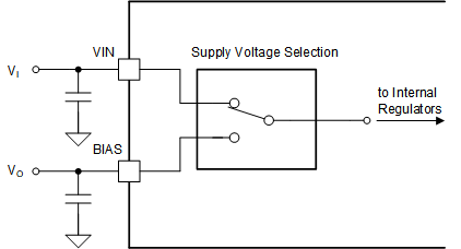
- The VIN pin is connected to the supply voltage. The BIAS pin is connected to VO. During start-up, that is as long as the output voltage is not higher than the supply switch-over threshold, the VIN supplies the internal regulators. Once VO is high enough, the supply current comes from the BIAS pin.
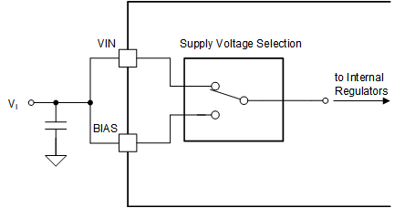
- Both the VIN pin and the BIAS pin are connected together to the input supply voltage. This configuration is often used in applications where the input supply voltage is usually lower or equal than the output voltage. As the BIAS pin is connected to the input voltage, the device has the full current capability of the internal regulators at low input voltages for start-up.
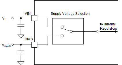
- The VIN is connected to the input supply voltage and the BIAS pin is connected to an auxiliary supply (for example, an existing 12V DC/DC converter). This configuration is commonly used at high voltage applications on the input and output voltages where the power dissipation over the integrated linear regulators must be further minimized.

Figure 8-9 VMAX Supply Scenario 1
 Figure 8-10 VMAX Supply Scenario 2
Figure 8-11 VMAX Supply Scenario 3
The VMAX does not directly select the highest voltage between the two supply pins BIAS and VIN. To achieve a minimum of power losses over the LDO the VMAX logic will decide what voltage is the closest one to the target supply VT(VCC,SUP) . The Table 8-1 gives an overview for the selection conditions:
| V(BIAS) | V(VIN) | VMAX supply |
|---|---|---|
| X | > VT+(VCC,SUP) && < V(BIAS) | VIN-PIN |
| > VT+(VCC,SUP) && < V(VIN) | X | BIAS-PIN |
| < VT-(VCC,SUP) | X | VIN-PIN |
| X | < VT-(VCC,SUP) | BIAS-PIN |
| > VT+(VCC,SUP) && > V(VIN) | > VT+(VCC,SUP) | VIN-PIN |
| > VT+(VCC,SUP) | > VT+(VCC,SUP) && > V(BIAS) | BIAS-PIN |
There is a FORCE_BIAS bit if it is 0b1 it lowers and prioritizes the switchover threshold for the BIAS pin. Intention is to support an external supply of nominal 5V for the VCC2 but still be able to start-up with the VIN supply if the sequencing if the external supply does not meet the start-up timing. The selection of the VCC2 supply follows this behavior:
- If the BIAS voltages is below the VT+(Force,BIAS) , then the VIN gets selected.
- If the BIAS voltage is above VT+(Force,BIAS) , then the BIAS gets selected regardless of VIN being above the VT+(VCC,SUP)