JAJSES8B October 2017 – November 2018 TPS2372
PRODUCTION DATA.
- 1 特長
- 2 アプリケーション
- 3 概要
- 4 改訂履歴
- 5 Pin Configuration and Functions
- 6 Specifications
-
7 Detailed Description
- 7.1 Overview
- 7.2 Functional Block Diagram
- 7.3
Feature Description
- 7.3.1 PG Power Good (Converter Enable) Pin Interface
- 7.3.2 CLSA and CLSB Classification, AUTCLS
- 7.3.3 DEN Detection and Enable
- 7.3.4 Internal Pass MOSFET and Inrush Delay Enable, IRSHDL_EN
- 7.3.5 TPH, TPL and BT PSE Type Indicators
- 7.3.6 AMPS_CTL, MPS_DUTY and Automatic MPS
- 7.3.7 VDD Supply Voltage
- 7.3.8 VSS
- 7.3.9 Exposed Thermal PAD
- 7.4
Device Functional Modes
- 7.4.1 PoE Overview
- 7.4.2 Threshold Voltages
- 7.4.3 PoE Startup Sequence
- 7.4.4 Detection
- 7.4.5 Hardware Classification
- 7.4.6 Autoclass
- 7.4.7 Inrush and Startup
- 7.4.8 Maintain Power Signature
- 7.4.9 Startup and Converter Operation
- 7.4.10 PD Hotswap Operation
- 7.4.11 Startup and Power Management, PG and TPH, TPL, BT
- 7.4.12 Using DEN to Disable PoE
-
8 Application and Implementation
- 8.1 Application Information
- 8.2
Typical Application
- 8.2.1 Design Requirements
- 8.2.2
Detailed Design Requirements
- 8.2.2.1 Input Bridges and Schottky Diodes
- 8.2.2.2 Protection, D1
- 8.2.2.3 Capacitor, C1
- 8.2.2.4 Detection Resistor, RDEN
- 8.2.2.5 Classification Resistors, RCLSA and RCLSB
- 8.2.2.6 Opto-isolators for TPH, TPL and BT
- 8.2.2.7 Automatic MPS and MPS Duty Cycle, RMPS and RMPS_DUTY
- 8.2.2.8 Internal Voltage Reference, RREF
- 8.2.2.9 Autoclass
- 8.2.2.10 Inrush Delay
- 8.2.3 Application Curves
- 9 Power Supply Recommendations
- 10Layout
- 11デバイスおよびドキュメントのサポート
- 12メカニカル、パッケージ、および注文情報
パッケージ・オプション
デバイスごとのパッケージ図は、PDF版データシートをご参照ください。
メカニカル・データ(パッケージ|ピン)
- RGW|20
サーマルパッド・メカニカル・データ
発注情報
7.4.9 Startup and Converter Operation
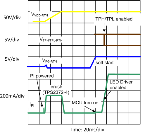
The internal PoE UVLO (Undervoltage Lock Out) circuit holds the hotswap switch off before the PSE provides full voltage to the PD. This prevents the downstream converter circuits from loading the PoE input during detection and classification. The converter circuits will discharge CBULK while the PD is unpowered. Thus V(VDD-RTN) will be a small voltage just after full voltage is applied to the PD, as seen in Figure 17. The PSE drives the PI voltage to the operating range once it has decided to power up the PD. When VVDD rises above the UVLO turn-on threshold (VUVLO_R, approximately 38 V) with RTN high, the TPS2372-3 and TPS2372-4 enables the hotswap MOSFET with inrush current limit (~200 mA for TPS2372-3 and ~335 mA for TPS2372-4) as seen in Figure 19. The PG pin is in low state while CBULK charges and VRTN falls from VVDD to nearly VVSS. PG output is maintained low during that time, to avoid additional loading between VVDD and VRTN that could prevent successful PD and subsequent converter start up. Once the inrush current falls about 10% below the inrush current limit, the PD current limit switches to the operational level (approximately 1.85 A for TPS2372-3 and approximately 2.2 A for TPS2372-4).
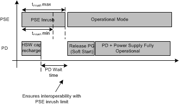
Additionally, as seen in Figure 19 once the inrush period duration has also exceeded ~81.5 ms, if IRSHDL_EN is open (this delay does not apply if connect to RTN), PG output becomes high impedance, allowing the downstream converter circuitry to start. In typical lighting applications, this allows a low power converter to start powering a microcontroller, which subsequently turns ON a high power LED driver. As seen in Figure 20, the converter soft-start introduces a slight additional delay before the transition to a higher power mode. TPH, TPL and BT outputs are enabled within tTPLHBT following PG going from low to open.
 Figure 19. Power Up and Start
  Figure 20. Power Up and Start
 If VVDD-VVSS drops below the lower PoE UVLO (VUVLO_F, ~32 V), the hotswap switch is turned off, but the PG output remains high impedance allowing the converter to continue operating until the converter's UVLO threshold is reached.