JAJSES8B October 2017 – November 2018 TPS2372
PRODUCTION DATA.
- 1 特長
- 2 アプリケーション
- 3 概要
- 4 改訂履歴
- 5 Pin Configuration and Functions
- 6 Specifications
-
7 Detailed Description
- 7.1 Overview
- 7.2 Functional Block Diagram
- 7.3
Feature Description
- 7.3.1 PG Power Good (Converter Enable) Pin Interface
- 7.3.2 CLSA and CLSB Classification, AUTCLS
- 7.3.3 DEN Detection and Enable
- 7.3.4 Internal Pass MOSFET and Inrush Delay Enable, IRSHDL_EN
- 7.3.5 TPH, TPL and BT PSE Type Indicators
- 7.3.6 AMPS_CTL, MPS_DUTY and Automatic MPS
- 7.3.7 VDD Supply Voltage
- 7.3.8 VSS
- 7.3.9 Exposed Thermal PAD
- 7.4
Device Functional Modes
- 7.4.1 PoE Overview
- 7.4.2 Threshold Voltages
- 7.4.3 PoE Startup Sequence
- 7.4.4 Detection
- 7.4.5 Hardware Classification
- 7.4.6 Autoclass
- 7.4.7 Inrush and Startup
- 7.4.8 Maintain Power Signature
- 7.4.9 Startup and Converter Operation
- 7.4.10 PD Hotswap Operation
- 7.4.11 Startup and Power Management, PG and TPH, TPL, BT
- 7.4.12 Using DEN to Disable PoE
-
8 Application and Implementation
- 8.1 Application Information
- 8.2
Typical Application
- 8.2.1 Design Requirements
- 8.2.2
Detailed Design Requirements
- 8.2.2.1 Input Bridges and Schottky Diodes
- 8.2.2.2 Protection, D1
- 8.2.2.3 Capacitor, C1
- 8.2.2.4 Detection Resistor, RDEN
- 8.2.2.5 Classification Resistors, RCLSA and RCLSB
- 8.2.2.6 Opto-isolators for TPH, TPL and BT
- 8.2.2.7 Automatic MPS and MPS Duty Cycle, RMPS and RMPS_DUTY
- 8.2.2.8 Internal Voltage Reference, RREF
- 8.2.2.9 Autoclass
- 8.2.2.10 Inrush Delay
- 8.2.3 Application Curves
- 9 Power Supply Recommendations
- 10Layout
- 11デバイスおよびドキュメントのサポート
- 12メカニカル、パッケージ、および注文情報
パッケージ・オプション
デバイスごとのパッケージ図は、PDF版データシートをご参照ください。
メカニカル・データ(パッケージ|ピン)
- RGW|20
サーマルパッド・メカニカル・データ
発注情報
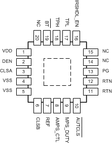
5 Pin Configuration and Functions
RGW Package
20-Pin VQFN
Top View

Pin Functions
| PIN | I/O | DESCRIPTION | |
|---|---|---|---|
| NAME | NO. | ||
| VDD | 1 | I | Connect to positive PoE input power rail. Bypass with 0.1 µF to VSS. |
| DEN | 2 | I/O | Connect a 24.9 kΩ resistor from DEN to VDD to provide the PoE detection signature. Pull DEN to VSS to disable the pass MOSFET during powered operation. |
| CLSA | 3 | O | Connect a resistor from CLSA to VSS to program the first classification current. |
| VSS | 4, 5 | — | Connect to negative power rail derived from PoE source. |
| CLSB | 6 | O | Connect a resistor from CLSB to VSS to program the second classification current. |
| REF | 7 | O | Internal 1.5 V voltage reference. Connect a 49.9kΩ_1% resistor from REF to VSS. |
| AMPS_CTL | 8 | O | Automatic MPS control. Connect a resistor with appropriate power rating (to support the MPS current) from AMPS_CTL to VSS to program the MPS current amplitude. Leave AMPS_CTL open to disable the automatic MPS function. |
| MPS_DUTY | 9 | I | MPS duty cycle select input, referenced to VSS, internally driven by a precision current source with voltage limited to less than ~5.5V. A resistor connected to VSS determines if the MPS duty cycle selected is either 5.4% (open), 8.1% (~60.4 kΩ) or 12.5% (short). |
| AUTCLS | 10 | I | Autoclass enable input. Internally pulled-up to 5.5 V internal rail during classification only, pulled down in other circumstances to minimize consumption. Pull low (to VSS) to enable the Autoclass function during classification. Leave open otherwise. |
| RTN | 11, 12 | — | Drain of PoE pass MOSFET. Return line from the load to the controller. |
| PG | 13 | O | Power Good output. Open-drain, active-high output referenced to RTN. |
| NC | 14, 15 | — | No connect |
| IRSHDL_EN | 16 | I | PSE inrush delay (~81.5 ms) enable, referenced to RTN, internally pulled-up to 5.5 V internal rail. Leave open to enable the inrush delay. |
| TPL | 17 | O | PSE allocated power outputs, binary coded. Open-drain, active-low outputs referenced to RTN. |
| TPH | 18 | O | |
| BT | 19 | O | Indicates that a PSE applying an IEEE802.3bt (Type 3 or 4) mutual identification scheme has been identified. Open-drain, active-low output referenced to RTN. |
| NC | 20 | — | No connect pin. Leave open. |
| Pad | — | — | The exposed thermal pad must be connected to VSS. A large fill area is required to assist in heat dissipation. |