JAJSMZ6 december 2021 UCC28781
PRODUCTION DATA
- 1
- 1 特長
- 2 アプリケーション
- 3 説明
- 4 Revision History
- 5 Pin Configuration and Functions
- 6 Specifications
-
7 Detailed Description
- 7.1 Overview
- 7.2 Functional Block Diagram
- 7.3
Detailed Pin Description
- 7.3.1 BUR Pin (Programmable Burst Mode)
- 7.3.2 FB Pin (Feedback Pin)
- 7.3.3 REF Pin (Internal 5-V Bias)
- 7.3.4 VDD Pin (Device Bias Supply)
- 7.3.5 P13 and SWS Pins
- 7.3.6 S13 Pin
- 7.3.7 IPC Pin (Intelligent Power Control Pin)
- 7.3.8 RUN Pin (Driver and Bias Source for Isolator)
- 7.3.9 PWMH and AGND Pins
- 7.3.10 PWML and PGND Pins
- 7.3.11 SET Pin
- 7.3.12 RTZ Pin (Sets Delay for Transition Time to Zero)
- 7.3.13 RDM Pin (Sets Synthesized Demagnetization Time for ZVS Tuning)
- 7.3.14 XCD Pin
- 7.3.15 CS, VS, and FLT Pins
- 7.4
Device Functional Modes
- 7.4.1 Adaptive ZVS Control with Auto-Tuning
- 7.4.2 Dead-Time Optimization
- 7.4.3 EMI Dither and Dither Fading Function
- 7.4.4 Control Law Across Entire Load Range
- 7.4.5 Adaptive Amplitude Modulation (AAM)
- 7.4.6 Adaptive Burst Mode (ABM)
- 7.4.7 Low Power Mode (LPM)
- 7.4.8 First Standby Power Mode (SBP1)
- 7.4.9 Second Standby Power Mode (SBP2)
- 7.4.10 Startup Sequence
- 7.4.11 Survival Mode of VDD (INT_STOP)
- 7.4.12
System Fault Protections
- 7.4.12.1 Brown-In and Brown-Out
- 7.4.12.2 Output Over-Voltage Protection (OVP)
- 7.4.12.3 入力過電圧保護 (IOVP)
- 7.4.12.4 FLT ピンの過熱保護 (OTP)
- 7.4.12.5 CS ピンの過熱保護 (OTP)
- 7.4.12.6 プログラム可能な過電力保護 (OPP)
- 7.4.12.7 ピーク電力制限 (PPL)
- 7.4.12.8 出力短絡保護 (SCP)
- 7.4.12.9 過電流保護 (OCP)
- 7.4.12.10 External Shutdown
- 7.4.12.11 Internal Thermal Shutdown
- 7.4.13 Pin Open/Short Protections
-
8 Application and Implementation
- 8.1 Application Information
- 8.2
Typical Application Circuit
- 8.2.1 Design Requirements for a 60-W, 15-V ZVSF Bias Supply Application with a DC Input
- 8.2.2 Detailed Design Procedure
- 8.2.3 Application Curves
- 9 Power Supply Recommendations
- 10Layout
- 11Device and Documentation Support
- 12Mechanical, Packaging, and Orderable Information
7.4.12.6 プログラム可能な過電力保護 (OPP)
過電力保護 (OPP) により、限られた時間だけ過電力状態で動作できるため、UCC28781 は一時的なピーク電力要件を持つ電力段の設計をサポートできます。次の図に示すように (IVSL 全体での VCST OPP 曲線)、VCST が OPP 曲線のスレッショルド電圧 (VCST(OPP)) を上回ると、160ms のタイマが開始されます。VCST が 160ms 連続して VCST(OPP) を上回ると、1.5 秒のタイマが開始され、コントローラはスイッチングを行わず障害状態を維持します。この長い回復時間により、持続的な過電力イベント中の平均電流が減少します。このシステムの利点として、高密度アダプタの熱ストレスの低減と、出力ケーブルの保護が挙げられます。
OPP 機能は、IVSL をライン・フィードフォワード信号として使用し、VBULK に応じて VCST(OPP) を変化させ、広いライン電圧範囲にわたって OPP のトリガ・ポイントを一定に保ちます。UCC28781 を使用すると、CS ピンと電流検出抵抗 (RCS) との間に接続された抵抗 (ROPP) を経由して、CS ピンにライン補償オフセット電圧を追加することで、OPP 曲線をプログラムできます。CS ピンから流れ出る内部電流源により、ROPP にオフセット電圧が発生します。この電流のレベルは、IVSL を固定ゲイン KLC で除算した値と等しくなります。ROPP が増加すると、High ラインで OPP トリガ・ポイントが低くなるため、ピーク磁化電流を低減して連続的に動作させることができます。
OPP 機能は、出力電圧のフィードフォワード信号として VVS を使用し、ライン依存の VCST(OPP) 曲線を 2 つの異なるセットに変更します。その結果、OPP トリガ・ポイントは広い出力電圧範囲にわたってより一貫性を維持できます。VVS > 2.5V での高い OPP スレッショルドには 2 つの個別リニア領域が含まれ、VVS < 2.4V での低い OPP スレッショルドには 1 つの個別リニア領域が含まれます。
OPP 曲線 (VCST(OPP1)) の最も高いスレッショルドである 0.6V は、VBULK(MIN) での RCS 値の決定に役立ちます。
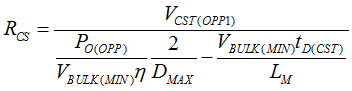
- ここで、PO(OPP) は OPP をトリガする出力電力です
- tD(CST) は、ピーク電流ループ内のすべての遅延の合計で、追加のピーク電流オーバーシュートに寄与します
tD(CST) は、ローサイド・ドライバの伝搬遅延、電流センス・フィルタ遅延 (ROPP × CCS)、内部 CS コンパレータ遅延 (tD(CS))、および QL の非線形容量遅延で構成されます。RCS が決定された後、ROPP を調整して、類似の OPP ポイントを最も高いラインに維持できます。OPP トリガ・ポイントをフルパワーから離れすぎた位置に設定すると、熱設計でより多くの課題が発生する可能性があることに注意してください。これは、対応するピーク電流が OPP スレッショルドをわずかに下回っている限り、コンバータはより多くの電力で連続的に動作するためです。
 図 7-43 IVSL 全体にわたる VCST OPP 曲線
 図 7-44 OPP のタイミング図