JAJU446A December   2017  – January 2022


  1.   概要
  2.   Resources
  3.   特長
  4.   アプリケーション
  5.   5
  6. System Description
    1. 1.1 Key System Specifications
  7. System Overview
    1. 2.1 Block Diagram
    2. 2.2 System-Level Description
    3. 2.3 Highlighted Products
      1. 2.3.1 Analog Signal Chain
        1. 2.3.1.1 LMH5401
        2. 2.3.1.2 LHM6401
        3. 2.3.1.3 BUF802
      2. 2.3.2 Clock
        1. 2.3.2.1 LMK61E2
        2. 2.3.2.2 LMK04828
        3. 2.3.2.3 LMX2594
      3. 2.3.3 Power
        1. 2.3.3.1 TPS82130
        2. 2.3.3.2 TPS7A84
    4. 2.4 System Design Theory
      1. 2.4.1 High-Speed, Low-Phase Noise Clock Generation
      2. 2.4.2 Channel-to-Channel Skew
      3. 2.4.3 Deterministic Latency
        1. 2.4.3.1 Importance of Deterministic Latency
      4. 2.4.4 Analog Front End
      5. 2.4.5 Multichannel System Power Requirement
      6. 2.4.6 Hardware Programming
  8. Circuit Design
    1. 3.1 Analog Input Front End
      1. 3.1.1 High-Input Impedance Buffer Implementation Using the BUF802
    2. 3.2 High-Speed Multichannel Clocking
    3. 3.3 Power Supply Section
      1. 3.3.1 DC-DC
        1. 3.3.1.1 How to Set 2.1-V Output Voltage
      2. 3.3.2 LDOs
  9. Host Interface
  10. Hardware Functional Block
  11. Getting Started Application GUI
  12. Testing and Results
    1. 7.1 Test Setup and Test Plan
    2.     44
    3. 7.2 SNR Measurement Test
    4. 7.3 Channel-to-Channel Skew Measurement Test
    5. 7.4 Performance Test Result
    6. 7.5 Multichannel Skew Measurement
    7. 7.6 49
  13. Design Files
    1. 8.1 Schematics
    2. 8.2 Bill of Materials
    3. 8.3 Altium Project
    4. 8.4 Gerber Files
    5. 8.5 Assembly Drawings
  14. Software Files
  15. 10Related Documentation
    1. 10.1 Trademarks
  16. 11About the Authors
    1. 11.1 Acknowledgment
  17. 12Revision History

Hardware Functional Block

Figure 5-1 shows the various hardware functional blocks of the TIDA-01022 design and the function of each block:

  1. A 12-V DC power supply input connector accepts the 9- to 12-V DC input to power the TIDA-01022
  2. Power supply section has switching regulator (DC-DC) and LDOs to generate multiple rails (1.1 V,
    1.9 V, 3.3 V, +2.5 V, and –2.5 V) from the 12-V input
  3. Four analog input channels which the designer can configure to accept 50-Ω single-ended or differential inputs
  4. AFE block contains combination of LMH5401+LMH6401, which accepts both AC and DC coupled inputs up to 1.5 GHz; optional transformer-coupled inputs are also available for an AC-coupled application up to 6 GHz
  5. FMC+ connector interfaces with TI High-Speed Data Capture card to the TSW14J56 using an FMC+ to FMC adapter PCB
  6. Clock subblock which contains high-performance clocking solution native to LMK04828, LMK2594, LMK00304, and LMK61E2 clocking devices
  7. Mini-USB interface connector helps to configure ADCs and clocking devices for various modes
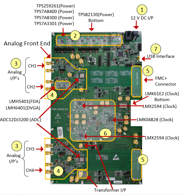
GUID-AEF91876-6EE6-40E6-9CA0-74FF447BB395-low.pngFigure 5-1 TIDA-01022 Hardware Functional Block