JAJU446A December 2017 – January 2022
- 概要
- Resources
- 特長
- アプリケーション
- 5
- 1 System Description
- 2 System Overview
- 3 Circuit Design
- 4 Host Interface
- 5 Hardware Functional Block
- 6 Getting Started Application GUI
- 7 Testing and Results
- 8 Design Files
- 9 Software Files
- 10Related Documentation
- 11About the Authors
- 12Revision History
2.4.3.1 Importance of Deterministic Latency
Any system that requires a feedback loop for digital capture or automatic process control is sensitive to latency variations. Latency variation affects the phase and gain margins and stability of a closed-loop control system. The presence of the delay potentially decreases stability and degrades the quality of control due to unavoidable gain reduction.
The JESD204B interface addresses these requirements and how to establish the deterministic latency of the link between a logic device and multiple data converters. Establishing this link is possible by using subclass 1 or 2. Depending on the subclasses, JESD uses SYSREF or the SYNC timing signal as a reference.
The ADC12DJ3200 device has a JESD204B interface feature that uses the DEV CLK and SYSREF signal to achieve multichannel synchronization and deterministic latency.
The subclass 1 requirements are as follows:
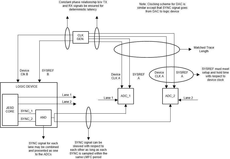
- Subclass 1 uses an external SYSREF signal to act as a common timing reference for multiple devices in a JESD204B system to achieve deterministic latency. The SYSREF signal is source synchronous to the device clock.
- For correct alignment, the SYSREF signal must meet the setup
and hold time requirements of the device clock and must be distributed to each
TX/RX device with a matched trace length and signal type relative to the device
clock (see Figure 2-5). The TX/RX device must specify the setup and hold time requirements of the
SYSREF signal with respect to the device clock at the input.
 Figure 2-5 JESD DEVCLK and SYSREF
Timing
 - The next requirement to meet is phase aligning the device clock
(sampling clock) and SYSREF signal with all data converter and logical devices.
This phase alignment requires trace length matching the DEVCLK and SYSREF
signals for all the devices. The SYNC signals from multiple logic devices
combine together as AND logic, which then transmit to the ADCs (see Figure 2-6).
 Figure 2-6 JESD System Level
DEVCLK, SYSREF, and SYNC Interface
 - Choose the appropriate elastic buffer release points in the JESD204B receivers to guarantee deterministic latency.
The TIDA-01022 reference design addresses these requirements for achieving deterministic latency and a minimum channel-to-channel skew. See the following resource for more details: JESD204B Deterministic Latency.