JAJU446A December 2017 – January 2022
- 概要
- Resources
- 特長
- アプリケーション
- 5
- 1 System Description
- 2 System Overview
- 3 Circuit Design
- 4 Host Interface
- 5 Hardware Functional Block
- 6 Getting Started Application GUI
- 7 Testing and Results
- 8 Design Files
- 9 Software Files
- 10Related Documentation
- 11About the Authors
- 12Revision History
7.5 Multichannel Skew Measurement
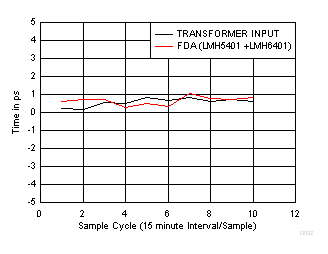
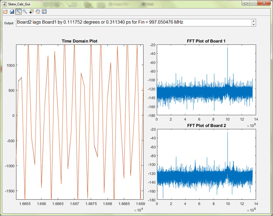
Table 7-2 lists the measured time skew between two channels (CH1 and CH3) of the TIDA-01022 design at room temperature with a 997-MHz input signal and at a sampling frequency of 2700 MHz. Evaluate this skew by calculating the phase difference between signals captured from each ADC. This measurement for both signal chain inputs and the measured time skew was less than 5 ps. Table 7-2 shows the skew measured between two channels for both the transformer input and FDA input path. Figure 7-10 shows the corresponding skew measurement data plot and Figure 7-11 shows the sampled signals in the time domain plot.
| SAMPLE CYCLE | TRANSFORMER COUPLING INPUT | FDA INPUT (LMH5401+6401) |
|---|---|---|
| 1 | 0.243 ps | 0.623 ps |
| 2 | 0.156 ps | 0.695 ps |
| 3 | 0.575 ps | 0.749 ps |
| 4 | 0.511 ps | 0.265 ps |
| 5 | 0.824 ps | 0.484 ps |
| 6 | 0.669 ps | 0.339 ps |
| 7 | 0.83 ps | 1.04 ps |
| 8 | 0.623 ps | 0.795 ps |
| 9 | 0.72 ps | 0.712 ps |
| 10 | 0.629 ps | 0.835 ps |
 Figure 7-10 Channel-to-Channel Measurement Plot
 Figure 7-11 Channel-to-Channel Skew Measurement GUI
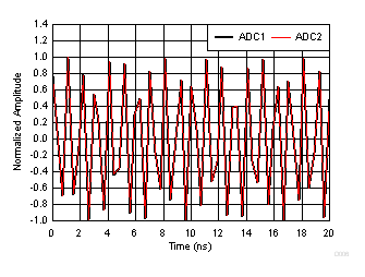
Figure 7-12 shows that the time domain measured plot of the ADC1 and ADC2 corresponds to CH1 and CH3 of the TIDA-01022 design.
 Figure 7-12 Sampled Signal at 997 MHz