SLOA284A january 2020 – may 2023 AFE5832 , AFE5832LP , ISO7741 , ISOW7841 , LM25037 , LM25180 , LM5180 , LM5181 , LM5181-Q1 , TX7316 , TX7332
2.1 TI HV Supply Architecture Using SEPIC Topology
This design implements a single stage architecture using only a single converter and a switch followed by two complementary output sections to generate the respective positive and negative HV rails. Custom made coupled inductors can benefit reduced energy losses due to leakage inductance, however, using uncoupled inductors helps meet the height requirements and better components choice [1]. The feedback is taken from positive output rail. Figure 2-2 shows the complete schematic of the design and Figure 2-3 shows the physical picture of the board highlighting the HV section.
 Figure 2-2 Schematic of the High Voltage
Circuit Design for Smart Probe
Figure 2-2 Schematic of the High Voltage
Circuit Design for Smart Probe Figure 2-3 Power Supply Board
Highlighting the HV Section
Figure 2-3 Power Supply Board
Highlighting the HV SectionTable 2-1 explains the component selection, and equations for the SEPIC power converter using LM3488 device.
| Parameter | Equations | Selected Components |
|---|---|---|
| Duty cycle | Equation 1. 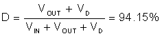 |
LM3488, which can reach a Duty cycle of 100%. |
| L1 (for minimum 40% current ripple ) | Equation 2. 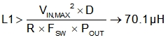 where, R is %ripple of input of current (0.4) |
100 µH (23% of current ripple), Isat = 1.2A, DCR = 0.377 Ω |
| L2, L3 (for minimum 40% current ripple) -> L3,L4 in Figure 2-2 | Equation 3. where, R is % ripple of input of current
(0.4)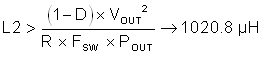 |
1000 µH (41 % of current ripple) Isat=80 mA, DCR=5.4Ω |
| MOSFET Q1 in Figure 2-2 | VSW(PEAK) = VIN +
VOUT+VD=86.28 =86.28V TOFF < 210 ns @ 250 kHz and D = 94.14% ; VGS(TH)< VIN |
CSD19538Q3A VDS,MAX = 100 V; RDS, ON = 58 mΩ VGS,TH = 3.2V; TOFF = 9 ns |
| CS2, CS3 -> C25, C35 in Figure 2-2 | VCS > VIN, MAX ; Equation 4. 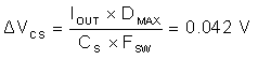 |
2.2 µF ; VDC=50V |
| D2, D3 -> D3, D6 | VIN+VOUT=85V - Schottky diode to minimize losses | STPS1150 ;VFORWARD = 0.78 V ; VRRM=150 V |
| COUT2, COUT3 ->C70,C232, C30, C31, C71, C233, C36 in Figure 2-2 | Equation 5. 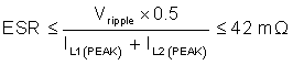 Equation 6. 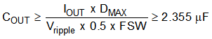 Vripple= 1% *Vout |
4 x 2.2 µF - VDC = 100 V |
| CIN -> C22, C23, C24 in Figure 2-2 | Equation 7.  |
2x 47 µf - 0.1 µF - VDC = 10 V |
| Compensation (RC,CC1 and CC2) R40, C27, C177 in Figure 2-2 | Equation 8. 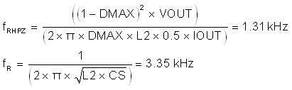 Equation 9. 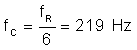 Equation 10. 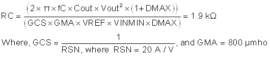 Equation 11. 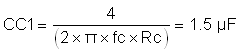 Equation 12. 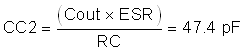 |
Rc = 4.70 kΩ - Cc1 = 0.1 µF - Cc2 = 0.1 µF |
The output of the SEPIC circuit is cascaded with a π filter followed by an emitter follower configuration (power filter) in order to minimize the AC ripple. The filter is built in order to provide an attenuation of 24.44 dB (see Equation 13) of the AC ripple as shown in Figure 3-3 through Figure 3-6 in Section 3.2.
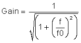
where f0 is the cut-off frequency of the RC filter and f is switching frequency of the input.