SLOA284A january 2020 – may 2023 AFE5832 , AFE5832LP , ISO7741 , ISOW7841 , LM25037 , LM25180 , LM5180 , LM5181 , LM5181-Q1 , TX7316 , TX7332
2 Design of high voltage circuit using SEPIC topology
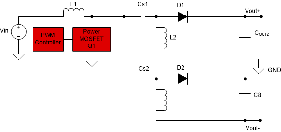
Figure 2-1 shows the generic schematic of the SEPIC topology. It uses three inductors: L1, L2 and L3. The three inductors can be wound on the same core since the same voltages are applied to them throughout the switching cycle and using a coupled inductor takes up less space on the PCB. However, they have to be custom made and may not be small in height, hence this solution uses uncoupled inductors. The capacitor CS1 and CS2isolate the input from the output and provides protection against a shorted load.
 Figure 2-1 SEPIC Topology Scheme
For detailed information on SEPIC, see the Designing A SEPIC Converter and the LM3488/-Q1 Automotive High-Efficiency Controller for Boost, SEPIC and Fly-Back DC-DC Converters. These documents refer to a coupled inductor approach, however the current solution adopts uncoupled inductors.