SLOA284A january 2020 – may 2023 AFE5832 , AFE5832LP , ISO7741 , ISOW7841 , LM25037 , LM25180 , LM5180 , LM5181 , LM5181-Q1 , TX7316 , TX7332
1 Introduction
Ultrasound imaging is widely used technique for diagnostic purpose. In addition to high-performance cart-based ultrasound systems, it is now possible to use a handheld device (smart probe) to accomplish high-quality ultrasound imaging. These smart probes leverage the power and resources of a mobile/tablet to process and display ultrasound images. A typical use case for these systems is to bring modern medical imaging technology to remote places, making the diagnostics faster. This small equipment is typically powered by battery (1S/2S), or from USB source. The data can be transferred over USB or Wi-Fi®.
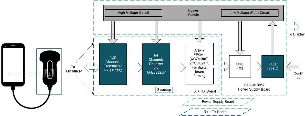
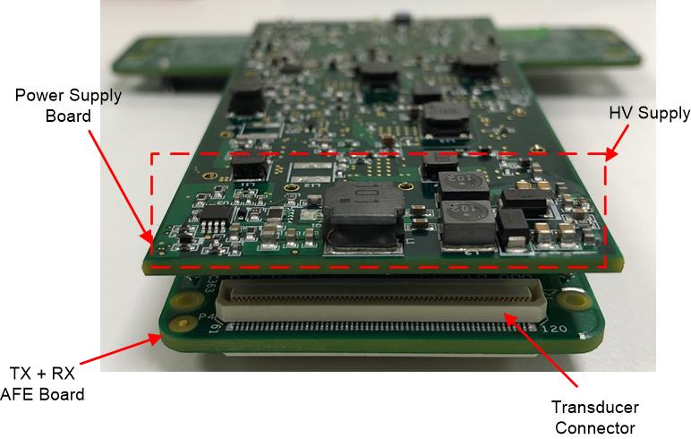
Figure 1-1 (left) shows a generic picture of such smart probe ultrasound scanner depicting a probe connected to a mobile device. Figure 1-1 (right) shows the system level block diagram of the smart probe, which includes transmit (TX) and receive (RX) analog front end (AFEs) for transmitting and receiving ultrasonic pulses and a FPGA to perform beam-forming. The whole setup is powered through the power supply board, consisting of DC-DC converters to generate point of load voltages, HV circuit for TX and USB controller for data and power management. This whole assembly of the analog front-end and power supply module is shown in Figure 1-2, where the different sections are highlighted in red.
 Figure 1-1 (left) Generic Smart Probe;
(right) System Block Diagram of Smart Probe Ultrasound Scanner
 Figure 1-2 Power Supply and TX+RX AFE
Boards
Figure 1-2 Power Supply and TX+RX AFE
BoardsThis application report focuses on the generation of compact, transformer less high-voltage supply for powering an ultrasound transmitter. This design generates programmable bipolar supply up to ±80V, from a very low input voltage (typically 5 V) in a single stage. Key constraints of size and height are met by using transformer-less SEPIC architecture. High efficiency of SEPIC architecture ensures low thermal footprint. This design also achieves <2% load regulation, fast transient response, and very low noise. The solution can be synchronized to an external clock in order to enable filtering of beat frequencies.
Table 1-1 below summarizes the design specifications of the high voltage circuit in the smart probe ultrasound scanner.
| Characteristics | Specifications |
|---|---|
| Input voltage range |
|
| Output voltage | Bipolar (from 10 V to 80 V @ 25 mA and -10 V to -80 V @ 25 mA), symmetrical loads |
| Peak Efficiency | 75% |
| Switching frequency | 250 kHz |
| Size (length x width) | 15 mm x 45 mm (single layer) |
| Height | < 5 mm |
| Output voltage regulation | <2% |
| Voltage symmetry with equal load on both rails | <1% |
| Output ripple | 0.1% of the output voltage |
| Synchronization to external clock frequency | Yes |