SLUP409B April 2022 – April 2024 TPS543320 , TPS543620 , TPS543820 , TPS62913 , TPS62916
- 1
- Abstract
- 1 Introduction
- 2 DC/DC Converters are Noisy
- 3 Power-Supply Output Voltage Ripple and Noise Degrade ADC Performance
- 4 Minimizing Low-Frequency Noise Requires Dedicated Low-Noise IC Technologies
- 5 Traditional Approaches to Reducing Ripple
- 6 Using Smaller Capacitors in Parallel
- 7 Larger Inductance
- 8 Adding a Feedthrough Capacitor
- 9 Adding a Ferrite Bead
- 10Layout Techniques
- 11Silicon Solutions
- 12Conclusions
9 Adding a Ferrite Bead
A more popular filtering technique is to use a ferrite bead to add a second-stage LC filter, as shown in Figure 23. A ferrite bead works well in a second-stage filter for several reasons. Ferrite beads are available with high enough inductance at frequencies less than 10MHz, so they can filter the output voltage ripple at the fSW and its harmonics. A ferrite bead’s increasing impedance from 100MHz to 1GHz enables the filtering of high-frequency switching noise from the rising and falling edges at the switching node.
Ferrite beads are available in small-sized standard packages, such as a 0603 package, and high-current ferrite beads have low DCR to minimize power loss. They are also relatively low cost, which is why designers use them often in systems to provide filtering.
When selecting a ferrite bead for power filtering, pay attention to the inductance saturation, which can reduce the inductance and filtering provided. To minimize the effect of saturation, choose a ferrite bead rated for two times the load current. If the power rail goes to multiple loads, you can use multiple ferrite beads, placing one before each load.
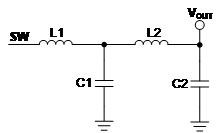 Figure 23 Two-stage LC filter.
When adding a second-stage LC filter to the output, one important goal is to keep the second stage’s resonance frequency (fLC2) well above the loop bandwidth of the regulator in order to minimize the impact of fLC2 on loop stability. A general recommendation is to keep fLC2 at least three times above the loop bandwidth. This consideration becomes especially important when using a regulator such as the TPS543620, which is designed for fast transient response – and as a result can have a relatively high loop bandwidth between one-tenth and one-fifth the switching frequency. With a 1-MHz switching frequency, the loop bandwidth is often greater than 100kHz.
There are two ways to design a second-stage filter to have a high resonance frequency:
- Select a ferrite bead with low inductance. Luckily, most high-current ferrite beads with low DCR also have low inductance.
- Keep the capacitance before the ferrite bead small. Minimizing this capacitance increases the second-stage resonance frequency because the fLC2 is set by the series combination of C1 and C2, as shown in :
When placing capacitors in series, if one capacitor is much smaller than the other, the combined series capacitance is closer to the smaller capacitance. Making C1 much smaller than C2 reduces the combined series capacitance and increases the second-stage resonance frequency. Equation 5 calculates the fLC2:
Adding a second-stage LC filter often requires damping in order to reduce the quality factor (Q). With too much Q, there will be peaking in the loop gain at fLC2, which can cause the loop gain to go above 0 dB and result in oscillations on the output voltage at fLC2. You can add a damping resistor to the circuit in two places:
- In parallel with the second-stage inductance.
- In series, with a capacitor added before the second-stage inductance.
The parallel damping method is simpler to implement but reduces the filtering provided, which is a significant trade-off. At higher frequencies, the parallel resistor will have a lower impedance than L2, causing high-frequency noise to pass through the resistor and bypass the inductor entirely. So in this example, we used series RC damping. Figure 24 shows the simplified circuit for this method.
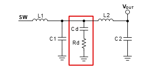 Figure 24 RC damping of the second-stage
filter.
Figure 24 RC damping of the second-stage
filter.Let’s go through the design methodology for selecting the resistor and capacitor values in the damping circuit. First, select capacitor value Cd to be ≥ C1. Next, select resistor value Rd so that the RC frequency is one-half fLC2, calculated with Equation 6:
Equation 6 only considers C1 because, as long as the first condition is met to select Cd ≥ C1, Rd will determine the impedance of the series combination of Rd and Cd at fLC2.
Figure 25 shows the schematic tested with the TPS543620 and a ferrite bead second-stage filter. The resonance frequency of the second-stage filter is approximately 300kHz. In addition to adding the second-stage filter, we changed the ramp to the 1-pF setting to reduce the loop gain by 6dB.
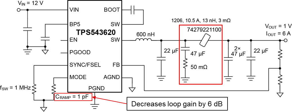 Figure 25 The TPS543620 EVM with a
ferrite bead second-stage filter.
Figure 25 The TPS543620 EVM with a
ferrite bead second-stage filter.Figure 26, Figure 27 and Figure 28 show the measurements as a result of adding the ferrite bead. In Figure 26, the ferrite bead clearly reduces the output ripple – both the ripple at the fSW and the high-frequency switching noise – to less than 10mVp-p. The ripple at the fSW is barely visible with the 10-mV-per-division voltage scale used in Figure 27. The FFT in Figure 28 clearly shows significant reductions in the peaks at each frequency, including reducing the peak at the 1-MHz fSW to almost one-tenth the original.
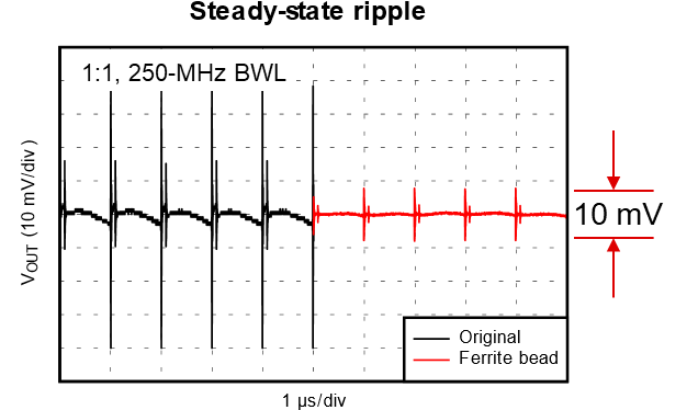 Figure 26 Ferrite bead output
ripple.
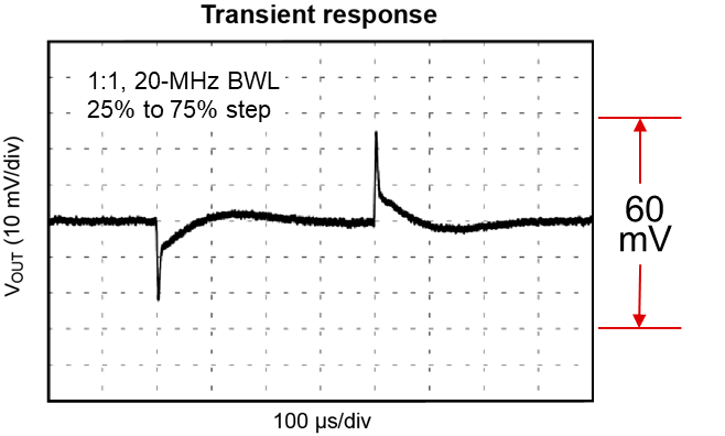 Figure 27 Ferrite bead transient
response.
 Figure 28 Ferrite bead output
FFT.
Figure 28 Ferrite bead output
FFT.The transient response is about the same, however, so the loop stability requires a closer look. Figure 29 shows the Bode plot with the ferrite bead added. There is a steep rolloff in the gain and phase from the second-stage filter at approximately 300kHz. The loop bandwidth is also very high at approximately 140kHz, which does not meet the requirement to have the second-stage filter resonance be three times the loop bandwidth. As a result, the gain margin is lower than the 10-dB typical design requirement, and the phase margin is lower as well. A low gain margin introduces a risk that circuit variations could result in oscillations on the output.
To improve the gain margin, you must either increase the second-stage resonance frequency or decrease the loop bandwidth. Increasing the second-stage resonance frequency will reduce the filtering, and in this case the ripple is already higher than the 200-µVp-p target. To avoid increasing the ripple, it’s better to decrease the loop bandwidth, but doing so will come with the trade-off of requiring more output capacitance to provide the same transient response performance. And with an internally compensated regulator such as the TPS543620, there is less flexibility in tuning the loop bandwidth, and the lowest loop gain setting is already set. Thus, in this case, reducing the loop bandwidth requires a modification of the output filter.
The second curve in Figure 29 shows the effect on loop stability with the first-stage inductance increased to 1.5µH. The loop bandwidth decreases to 60kHz and the gain margin improves to 13dB.
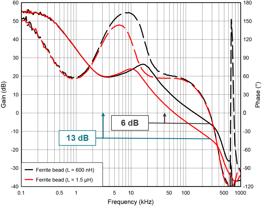 Figure 29 Bode plot with a ferrite bead
filter.
Figure 29 Bode plot with a ferrite bead
filter.A sub-1-mV ripple at the fSW and its harmonics is possible when using a ferrite bead to filter the output because a ferrite bead effectively filters the ripple at the fsw and higher. The trade-off is that using a ferrite bead can result in more components (such as damping components) and design time to compensate the loop. Adding in a ferrite bead can also limit the maximum loop bandwidth (which degrades transient response performance) and results in some conduction losses in its DCR.