SLUP409B April 2022 – April 2024 TPS543320 , TPS543620 , TPS543820 , TPS62913 , TPS62916
- 1
- Abstract
- 1 Introduction
- 2 DC/DC Converters are Noisy
- 3 Power-Supply Output Voltage Ripple and Noise Degrade ADC Performance
- 4 Minimizing Low-Frequency Noise Requires Dedicated Low-Noise IC Technologies
- 5 Traditional Approaches to Reducing Ripple
- 6 Using Smaller Capacitors in Parallel
- 7 Larger Inductance
- 8 Adding a Feedthrough Capacitor
- 9 Adding a Ferrite Bead
- 10Layout Techniques
- 11Silicon Solutions
- 12Conclusions
3 Power-Supply Output Voltage Ripple and Noise Degrade ADC Performance
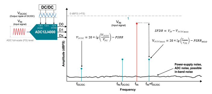
It is difficult to estimate the acceptable output voltage ripple and noise for a power-supply rail without a deeper understanding of the ADC and its performance. Figure 3 shows the output frequency spectrum of an ADC.
 Figure 3 Power-supply spur modulation,
with an ADC input signal decreasing the SFDR.
Figure 3 Power-supply spur modulation,
with an ADC input signal decreasing the SFDR.In the best case, the output voltage spectrum should show a single line at the input frequency of the ADC. When a power supply connects to an ADC, the frequency of the output voltage ripple modulates with the ADC frequency, generating sidebands above and below the ADC input signal frequency. The larger these sidebands are in amplitude, the lower the SFDR. Equation 1 calculates the amplitude of the modulated spur:
where VFS is the full-scale level of the ADC, VDCDC is the peak-to-peak output voltage ripple of the DC/DC converter and PSRRMOD is the power-supply rejection of the ADC.
The spur needs to be lower than the SFDR of the ADC. PSRRMOD is the attenuation of the power-supply ripple to the amplitude of the modulated spur in the ADC output spectrum. PSRRMOD is not usually specified in ADC data sheets, but is possible to characterize. If characterization is not possible, then you can conservatively estimate PSRRMOD by taking 20 dB for the PSRRMOD of the ADC, plus 10 dB for additional printed circuit board (PCB) power-supply bypass capacitor attenuation, for a total system board attenuation of 30 dB. Equation 2 calculates the acceptable DC/DC converter output voltage ripple:
With Equation 2 setting an SFDR of –100 dB as a target, VDCDC_MOD needs to be –100 dB as well. The typical high-speed ADC full-scale level specified in the ADC data sheet is 725 mV. Having a target output voltage ripple of <200 µVpp for the DC/DC converter proves to be a good value and does not degrade the ADC’s SFDR.