SLUP409B April 2022 – April 2024 TPS543320 , TPS543620 , TPS543820 , TPS62913 , TPS62916
- 1
- Abstract
- 1 Introduction
- 2 DC/DC Converters are Noisy
- 3 Power-Supply Output Voltage Ripple and Noise Degrade ADC Performance
- 4 Minimizing Low-Frequency Noise Requires Dedicated Low-Noise IC Technologies
- 5 Traditional Approaches to Reducing Ripple
- 6 Using Smaller Capacitors in Parallel
- 7 Larger Inductance
- 8 Adding a Feedthrough Capacitor
- 9 Adding a Ferrite Bead
- 10Layout Techniques
- 11Silicon Solutions
- 12Conclusions
11 Silicon Solutions
The TPS62913 and TPS62916 are low-ripple and low-noise buck converters that use the techniques we’ve previously described as well as low-noise techniques borrowed from low-noise LDOs. These devices support-input voltages from 3V to 17V and output voltages from 0.8V to 5.5V. This product family contains five device variants that can support output currents from 2A to 8A."
While the efficiency of the TPS62913 and TPS62916 by itself is quite high, it is possible to further improve system-level efficiency if you consider removing the LDO for many applications. Until now, how to reduce ripple through external design techniques has been discussed. Now, the integration of features into a buck converter like the TPS62913 to reduce noise and ripple will be discussed. Figure 33 and Figure 34 show a typical schematic for generating a low-noise 3.3-V supply using the TPS62913 and TPS62916, respectively.
 Figure 33 TPS62913 typical
schematic.
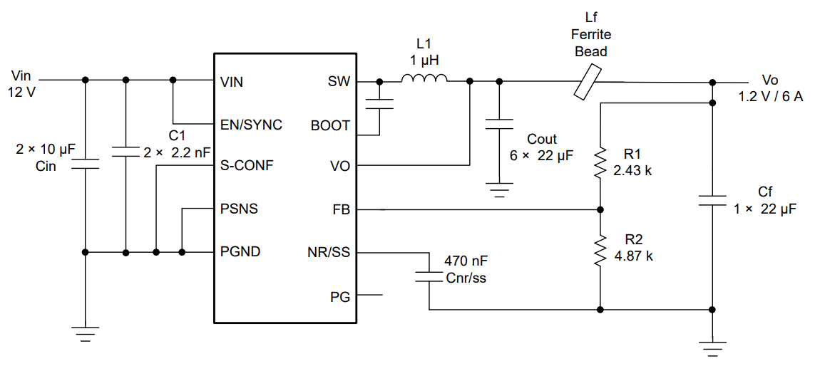 Figure 34 TPS62916 typical
schematic.
Figure 34 TPS62916 typical
schematic.The first technique integrated into the TPS62913 uses a 2.2-MHz switching frequency in conjunction with a larger-than-normal inductance for the first LC filter. The combined result of this high switching frequency with a 2.2-µH inductor is a reduction in the di/dt ripple.
This reduction in di/dt also affects the transient response, though, so using a large inductance is best suited for applications where the load is fairly steady, such as clocks and PLLs. The larger inductance and higher switching frequency may also work for 1.8-V noise-sensitive ADCs, digital to analog converters and AFE rails. For core power, it will depend on the load transient requirements.
The second feature used in both devices is an integrated ferrite bead filter compensation. The first LC filter loop uses the VO pin to sense the first LC output, with a crossover frequency of approximately 130 kHz for the example shown. The device uses the feedback pin to sense the output voltage after the ferrite bead filter through a resistor divider. Using this feedback pin with internal ferrite bead filter compensation (which is much slower than the first LC compensation) enables stable operation of the circuit and eliminates the ferrite bead filter problems discussed earlier.
SMA connectors can measure the output voltage ripple before and after the second LC filter. Figure 35 highlights the ripple at the first LC filter in red and highlights the ripple after the ferrite bead filter in blue.
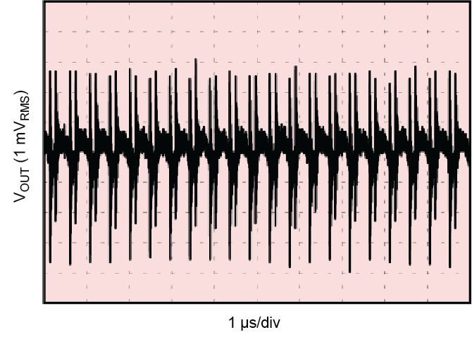
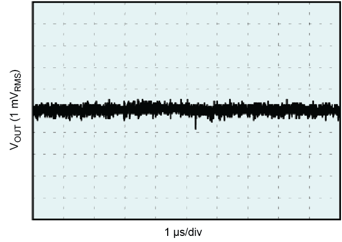 Figure 35 Output voltage ripple in the
time domain before and after the ferrite bead filter.
Figure 35 Output voltage ripple in the
time domain before and after the ferrite bead filter.In addition to the time-domain measurements, it is useful to use a spectrum analyzer to generate an FFT plot, as shown in Figure 36.
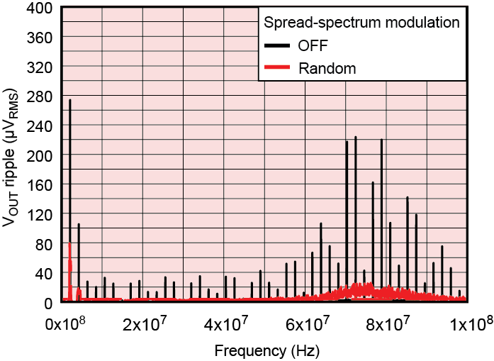
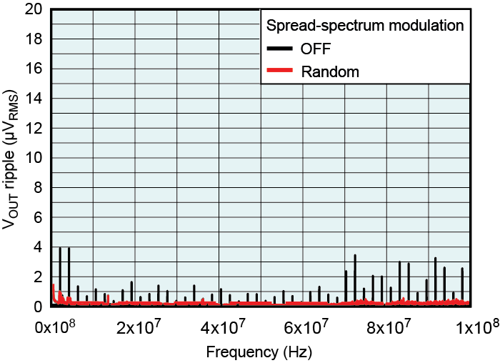 Figure 36 Output voltage ripple in the
frequency domain before and after the ferrite bead filter.
Figure 36 Output voltage ripple in the
frequency domain before and after the ferrite bead filter.We generated these plots using a 10-kHz bandwidth from 500 kHz to 100 MHz to show the frequency components of the ripple that you cannot distinguish when looking at the time-domain ripple measurement on an oscilloscope.
As discussed previously, a ferrite bead filter effectively filters the fundamental fSW and the higher-frequency components. Both the TPS62913 and TPS62916 have an integrated ferrite bead filter compensation that works for a wide variety of ferrite beads up to a 50-nH inductance. Note that the output voltage is sensed by the feedback pin resistor divider after the ferrite bead filter, which helps with DC regulation if there is an output voltage drop caused by the ferrite bead resistance. The VO pin feedback achieves loop stability for the primary LC filter. These two separate feedback loops (VO and FB) ensure stability and regulation. The TPS62913 also includes spread-spectrum options that, when enabled, can further reduce the ripple.
There are many potential sources of noise (100Hz to 100kHz), including the bandgap, error amplifier, feedback divider, current-sense amplifier and oscillator. By far, the biggest contributor to noise is the bandgap, so filtering the voltage reference with an external capacitor yields significantly lower integrated noise. The TPS62913 and TPS62913 integrate a noise-reduction capacitor with a soft-start function, similar to many low-noise LDOs. After completing soft start, the soft-start capacitor becomes a noise-reduction capacitor. A 470-nF soft-start noise-reduction capacitor results in a 5-ms soft-start time and a 16.7-µVRMS integrated noise figure from 100Hz to 100kHz. The integrated error amplifier and current-sense amplifier in the TPS62913 and TPS62916 are optimized for low-noise behavior as well.
Keeping the external feedback resistors fairly low in value helps to reduce the impedance on the feedback pin and minimize any noise contribution. Using lower-value resistors will burn slightly more power, but this is usually an acceptable trade-off, since the loads are fairly constant and low quiescent current is not necessary for standby modes. The power savings gained by eliminating the LDO more than make up for the higher light-load current.
A high-performance ADC used in test and measurement applications demonstrates the effectiveness of these silicon techniques. The Powering Sensitive Noise ADC Designs with the TPS62913 Low-Noise Buck Converter reference design, shown in Figure 37, uses four low electromagnetic interference switching converters, using the LMS3635M step converter with three low-noise LDOs and ferrite beads.
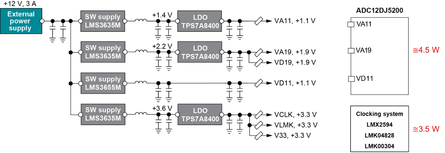 Figure 37 Original ADC design with
switching converters and LDOs.
Figure 37 Original ADC design with
switching converters and LDOs.Figure 38 shows how the TPS62913 simplifies this design by eliminating the LDOs.
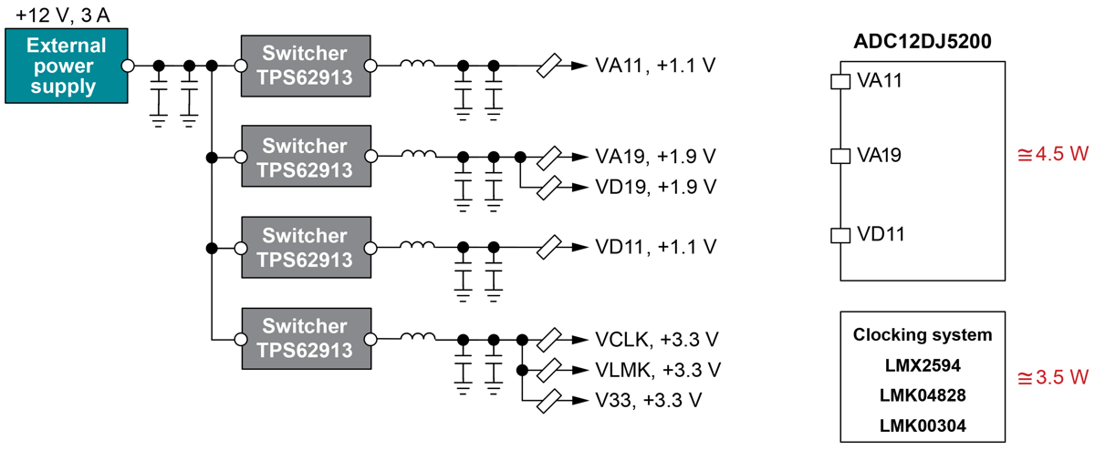 Figure 38 ADC design using the TPS62913
converter without LDOs.
Figure 38 ADC design using the TPS62913
converter without LDOs.In the designs discussed in Figure 37 and Figure 38, the VA11 and VD11 rails are the most noise sensitive, so we used separate switchers for each rail. The clocking circuit implements individual ferrite bead filters on all three 3.3-V rails for clocking power, with the feedback sense point connected to the highest current rail. This approach enables a single device to supply multiple rails with low noise and low ripple while maintaining the best load regulation.
Figure 39 shows how the TPS62913 provides a much smaller solution size by eliminating the LDOs. In addition to the size reduction, eliminating the thermal loss of the LDOs results in a 1.5-W power reduction, which reduces total system power by 15%. Thermal management also becomes easier, since the hottest parts on the original board were the LDOs.
 Figure 39 Size and power savings
comparison.
Figure 39 Size and power savings
comparison.Figure 40 compares the traditional approach with LDOs and a clock vs. The TPS62913 approach with no LDOs powering the ADC and clock for SNR, SFDR, noise spectral density and PSRRMOD. The low-noise features of the TPS62913 enable the powering of noise-sensitive rails of the clock and ADC without an LDO while closely meeting the performance specifications listed on the ADC12DJ5200RF 10.4-GSPS Single-Channel or 5.2-GSPS Dual-Channel, 12-bit, RF-Sampling Analog-to-Digital Converter (ADC) Data Sheet.
The SNR achieves results within half a decibel of the LDO implementation and close to the performance listed on the data sheet.
The SFDR also achieves results within half a decibel of the LDO implementation.
The noise spectral density shows performance within 1 dB of the LDO implementation.
And finally, the PSRRMOD shows no in-band noise vs. the LDO implementation. Since the TPS62913 solution switches at 1 MHz, even the spur at 600 kHz from the previous DC/DC converter is eliminated.
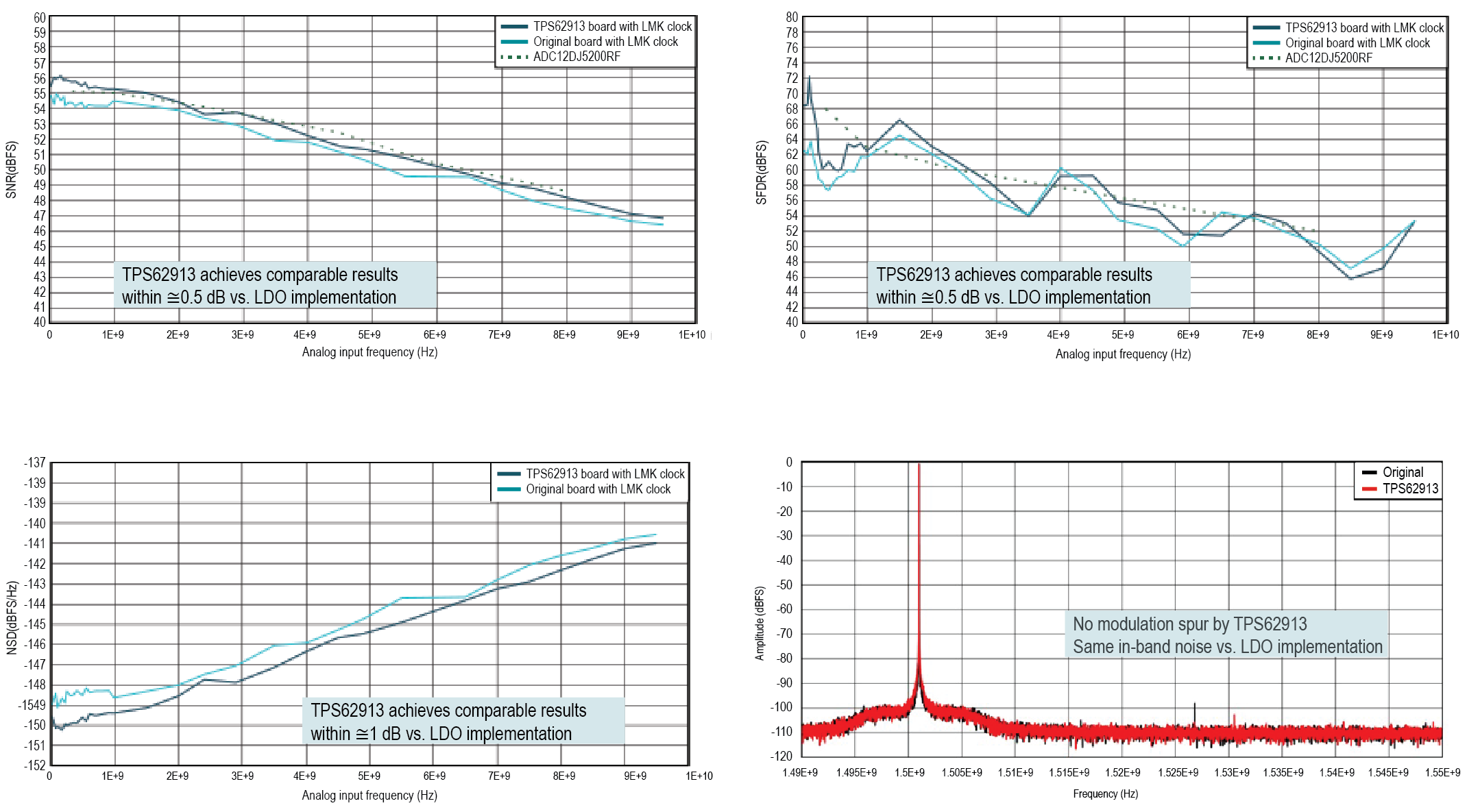 Figure 40 Performance comparisons for
SNR, SFDR, noise spectral density and PSMR.