SLUP409B April 2022 – April 2024 TPS543320 , TPS543620 , TPS543820 , TPS62913 , TPS62916
- 1
- Abstract
- 1 Introduction
- 2 DC/DC Converters are Noisy
- 3 Power-Supply Output Voltage Ripple and Noise Degrade ADC Performance
- 4 Minimizing Low-Frequency Noise Requires Dedicated Low-Noise IC Technologies
- 5 Traditional Approaches to Reducing Ripple
- 6 Using Smaller Capacitors in Parallel
- 7 Larger Inductance
- 8 Adding a Feedthrough Capacitor
- 9 Adding a Ferrite Bead
- 10Layout Techniques
- 11Silicon Solutions
- 12Conclusions
7 Larger Inductance
Another filtering technique to reduce the output ripple is to increase the inductance. Increasing the inductance reduces the amount of ripple current that the output capacitors need to filter. Additionally, the inductor and the parasitic inductance in the output capacitor network form a voltage divider from the switch node to the output. Increasing the inductance increases the inductive voltage divider ratio, resulting in less output ripple divided down from the switch node.
This approach was tested with the TPS543620 by increasing the inductance of the schematic in Figure 5 from 600nH to 2.2µH, which reduces the transient currents (di/dt) in the inductor by a factor of 3.7.
As a result of this increase in inductance, we increased the compensation setting for the TPS543620 (CRAMP) to the 4-pF ramp in order to increase the loop gain by 6 dB. Figure 14, Figure 15 and Figure 16 show the measurements as a result of this change.
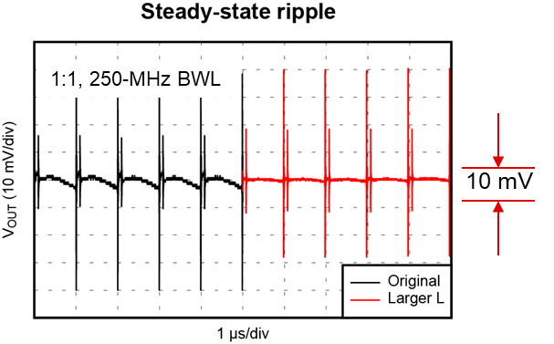
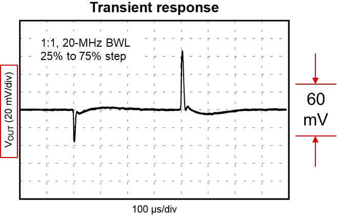
Figure 14 shows the reduced ripple at the fSW, but the high-frequency content is about the same as before. In Figure 15, however, the reduced di/dt has degraded the transient performance. The peak-to-peak transient response is nearly two times larger with the same step, necessitating an increase in the voltage scale in the waveform to 20mV per division in order to fit the full peak-to-peak voltage on the graph. Figure 16 shows a reduction of the fundamental peak at the 1-MHz fSW and its harmonics to one-sixth the original.
 Figure 14 Larger inductor output
ripple.
 Figure 15 Larger inductor transient
response.
 Figure 16 Larger inductor output
FFT.
Figure 16 Larger inductor output
FFT.Increasing the inductance is a simple and effective change for reducing the output voltage ripple, but that approach comes with some trade-offs that could be significant. A higher inductance typically means a larger inductor with higher direct current resistance (DCR), which results in a larger PCB footprint, increased cost and more conduction losses. The lower di/dt slows down the transient response. And finally, increasing the inductance provides little to no added filtering at frequencies greater than 100 MHz because of the parasitic capacitance of the inductor.